Help Center  
Sending a message
Open Hours:9:00-21:00 (GMT+8)
Service hotlines
+86-755-27218592

9:00 -18:00, Mon. - Fri. (GMT+8)

9:00 -12:00, Sat. (GMT+8)

(Except Chinese public holidays)

X

Assembly Enquiry

Add gerber File

Instant Quote

Add gerber File

Our Capabilities

Design Cases

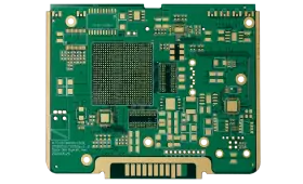
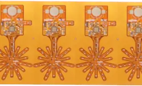
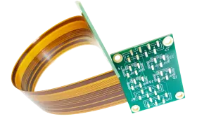
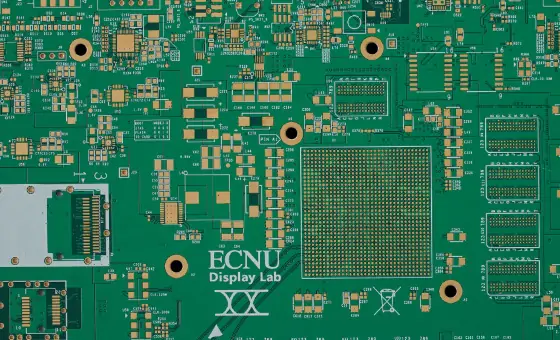
We have a variety of product cases for your reference.

Industrial Robot PCB
Industrial Control PCB
Industrial Robot PCB
Medical Device PCB
Automotive PCB
Consumer Electronics PCB
Smart Home PCB

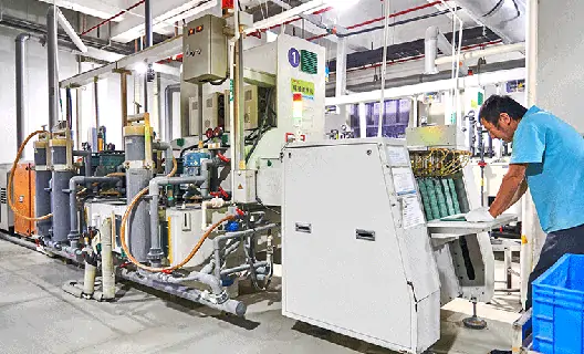
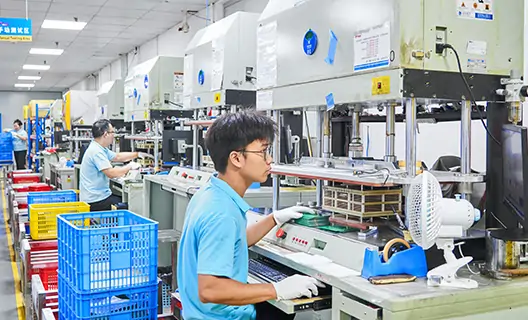
Key PCB Manufacturing Processes

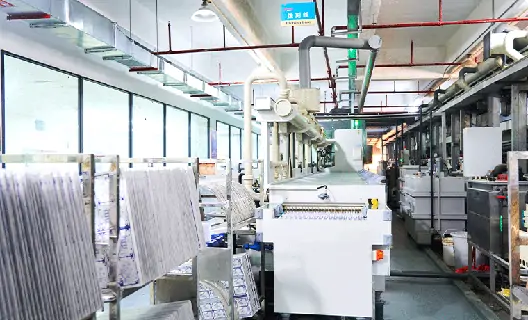
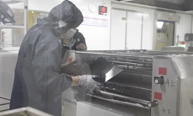
Each step in the PCB manufacturing process adheres to strict inspection standards.
01File Review
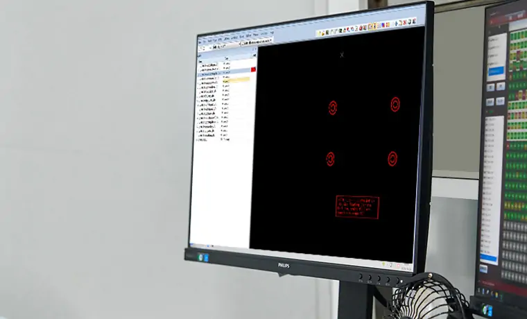
Before production begins, we perform a comprehensive review of the design files provided by the customer (e.g., Gerber files) to ensure the integrity and manufacturability (DFM) of the PCB design. We also generate the necessary drill files, artwork files, and other production tools to ensure the accuracy and efficiency of subsequent processes.

02Inner Layer Fabrication

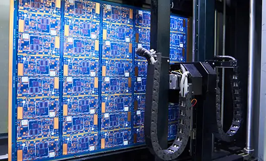
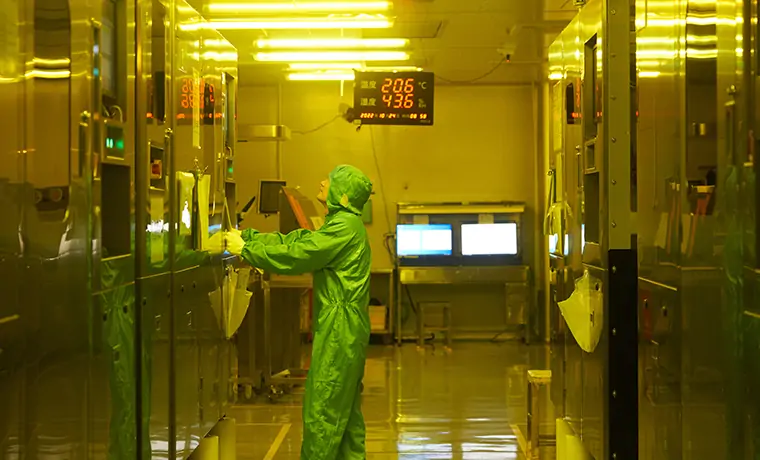
For multi-layer PCB production, inner layer fabrication is a crucial step. We use advanced photo imaging technology to precisely transfer the circuit pattern onto the copper-clad laminate, and chemically etch away excess copper to form the circuit pattern. AOI (Automated Optical Inspection) is then used to inspect 100% of the inner layer, ensuring no open circuits, shorts, or other defects.

03Drilling

We use high-precision CNC drilling machines to process through-holes, blind vias, and buried vias, ensuring precise hole locations and dimensions that meet design requirements. The cleaning process after drilling further removes residue inside the holes, laying a solid foundation for the subsequent via plating process.

04Through-Hole Plating

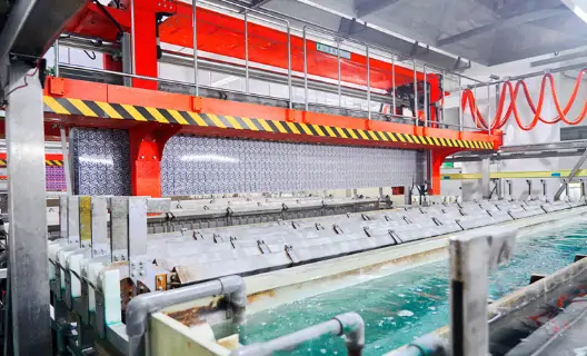
Through-hole plating is a core process for achieving interlayer electrical connections. We first use chemical copper deposition to deposit a conductive copper layer inside the holes, followed by electroplating to thicken the copper layer, ensuring the reliability of electrical performance and mechanical strength. We strictly control the plating thickness to meet international standards.

05Outer Layer Fabrication

The outer layer fabrication determines the final circuit pattern of the finished PCB. We use high-precision exposure technology and electroplating to transfer the circuit pattern onto the outer layers, followed by etching to remove excess copper foil. Once complete, all outer layers undergo AOI inspection again to ensure every PCB meets the design requirements.

06Solder Mask Application

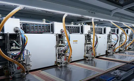
Applying a solder mask to the PCB surface effectively protects the circuit areas and prevents soldering short circuits. We use automated coating equipment and precise exposure technology to ensure the solder mask ink is evenly applied, with precise opening for the soldering areas. After high-temperature curing, the solder mask layer provides excellent wear resistance and insulation properties.

07Surface Finish

To enhance the solderability of the PCB and protect exposed surfaces, we offer a variety of surface finish processes, including Hot Air Solder Leveling (HASL), Electroless Nickel Immersion Gold (ENIG), Immersion Tin, and OSP (Organic Solderability Preservative). Each process meets international standards to fulfill different application requirements.

08Electrical Testing

Before shipment, each PCB undergoes a comprehensive electrical test, including continuity and insulation checks. We use advanced flying probe or bed-of-nails test equipment to ensure that all electrical connections meet the design requirements, providing customers with stable and reliable products.

09Final Inspection

Once production is complete, we conduct a final inspection of the PCB's appearance and functionality to ensure there are no defects.

10Packaging

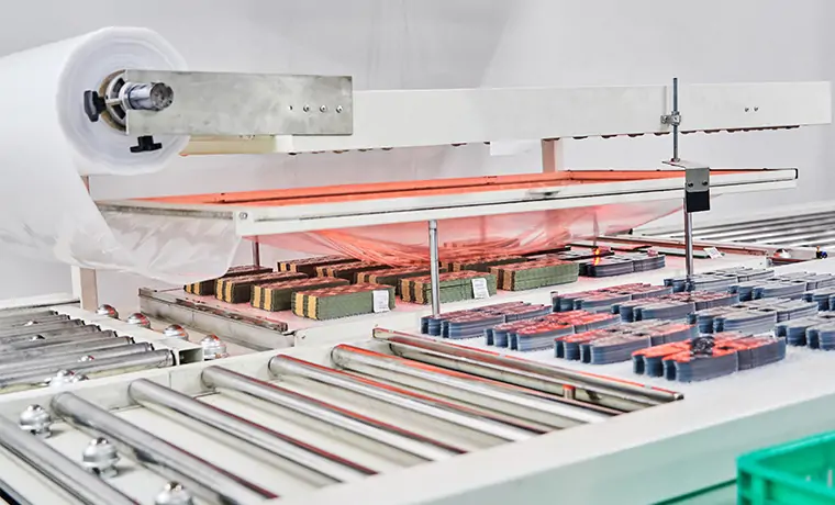
The PCBs are then packaged using anti-static bags, foam, and other materials to protect them from electrostatic discharge and physical damage. Finally, the PCBs are sealed in protective bags, labeled, and packed in outer cartons with cushioning materials to ensure safety and stability during transportation.
X

How to Place an Order and Request a Quote


  • Upload Files

    Submit your Gerber files, BOM (Bill of Materials), and any project-specific requirements to us.

  • Technical Review

    Our engineering team will review your files and verify technical specifications

  • Receive Quote

    Get a detailed quote including pricing, lead time, and shipping options.

  • Confirm Order

    Review and confirm your order details, then proceed with payment to start production.
View Video Quote Process > Get an Instant Quote Now

Why Choose PCBasic as Your Partner?

About Us

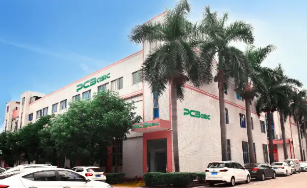
Established in Shenzhen, China, in 2011, PCBasic boasts more than 15 years of hard work and innovation in the field of PCB & PCBA manufacturing. The considerable expertise in printed circuit boards and decades of industrial experience grant PCBasic the confidence and strength to overcome challenges and deliver the best-in-class PCB & PCBA solutions, making it one of the leading PCB & PCBA manufacturers around the globe.

Learn More
  • Quality Focus

    Strictly comply with ISO9001, IATF16949, and ISO13485 standards.

  • High-Speed Delivery

    Rapid delivery for small batch products--within 24 hours at the fastest.

  • Advanced Technology

    PCBasic is equipped with a professional R&D team and possesses a self-invented intelligent production management system.

  • Best Purchase Experience

    No MOQ, even can get PCBs free!

  • Best Value for Money

    With multiple supply chains, PCBasic can offer the best quality at the most competitive prices.

  • Top After-Sales Service

    PCBasic guarantees a full refund in case of quality problems.

  • 100+

    Serves more than 100 countries around the world

  • 120000+

    Has over 120,000 global customers in PCB prototype assembly service

  • 1000+

    Handles 1000+ pieces of PCB design and layout order documents every day

  • 96.15%

    Boasts 96.15% on-time delivery in PCBA service

PCB Order List Your order is Process!
80706

Last 30 days

CustomerTimeQuantityDeliveryAmount
  • 10-22500pcs 55h $ 2450
  • 10-22120pcs 48h $ 1550
  • 10-22100pcs 43h $ 1450
  • 10-22150pcs 34h $ 1200
  • 10-22500pcs 55h $ 1700
  • 10-22500pcs 55h $ 2450
  • 10-22120pcs 48h $ 1550
  • 10-22100pcs 43h $ 1450
  • 10-22150pcs 34h $ 1200
  • 10-22500pcs 55h $ 1700

I highly recommend this company for their outstanding PCBA processing services. The anti-static precautions and detailed proofing process are impressive, resulting in high-quality and reliable products.

Sneha Singh 2024-08-08

The quality assurance process here is rigorous. The small-batch trial production helped us ensure that the final products were flawless. We appreciate their dedication to quality and precision.

Camille Dupont 2024-10-09

Their service is superior in every aspect. From the initial consultation to the final product delivery, everything was handled with the utmost professionalism. The PCBA process was smooth and efficient.

Alexander White 2024-08-07

Samples have been tested and are very stable, further cooperation will be launched. The performance and reliability of the boards exceeded our expectations. Looking forward to a long-term partnership.

William Anderson 2024-08-07

The attention to electrostatic protection during PCBA processing is commendable. Our components are always handled with utmost care, ensuring the integrity and functionality of our products. Highly recommend for anyone needing precise and professional PCBA services.

Maria Oliveira 2024-08-03

We were impressed by the thorough proofing process before mass production. The small-batch trial runs allowed us to identify and rectify potential issues early, ensuring a flawless final product. The quality and attention to detail are unparalleled.

John Smith 2024-08-08

Since PCBA processing often involves a variety of electrostatic sensitive electronic components and some processing techniques that have certain requirements for electrostatic protection, certain anti-static requirements are required in PCBA processing.

Anti-static 2024-07-30

irst, let's look at what PCB proofing is. Proofing, as the name suggests, is a small-batch trial production before mass production. Only when the proofing passes the inspection standards, can the mass product be released with peace of mind. This method av

PCB Prototyping 2024-08-01

Prints arrived in good condition. Are thereadditional costs for a follow-up order? or isthat a bit cheaper. 25 or 50 pieces?

Prints arrived 2024-08-02
Blog

Product Inspection Certificates

More Than 100+ Patent Certificates

ISO 9001:2015

ISO 9001:2015

pcba manufacturer with 13485 certificate

ISO 13485:2016

IATF 16949

IATF 16949

CCC

CCC

CE

CE

FCC

FCC

FCC

ISO 14001 : 2015

FCC

ISO 45001 : 2018

Get an Instant Quote Now

E-mail

Quote

0.563738s