Global high-mix volume high-speed PCBA manufacturer
9:00 -18:00, Mon. - Fri. (GMT+8)
9:00 -12:00, Sat. (GMT+8)
(Except Chinese public holidays)
Global high-mix volume high-speed PCBA manufacturer
9:00 -18:00, Mon. - Fri. (GMT+8)
9:00 -12:00, Sat. (GMT+8)
(Except Chinese public holidays)
HomePage > Blog > Knowledge Base > PCBA Test: A Comprehensive Guide to PCB Assembly Testing
Quality control is crucial for printed circuit board assembly (PCBA). A single PCBA test defect can negatively impact product performance and longevity. This can damage a company's reputation and lead to costly repairs or recalls.
According to a recent study, poor quality can cost over 40% of annual sales in the PCB manufacturing industry. Interestingly, the study also found that even Three Sigma quality-level operating companies spend nearly 25% of their yearly revenue remediating poor quality costs.
With growing product complexity and tighter margins, circuit board testing is more vital than ever. From simple in-circuit tests to complex system-level validation, the correct testing procedures can uncover issues before they reach customers. When implemented strategically, testing pays for itself by reducing post-production problems.
Read on as we delve into the most effective PCBA testing methods to help ensure quality products and avoid costly mistakes.
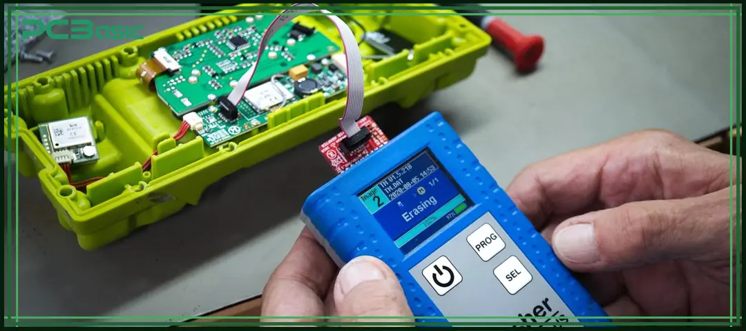
The printed circuit board assembly (PCBA) test is a quality control process used in electronic manufacturing. A PCBA refers to the assembled printed circuit board found in virtually all electronic devices, such as computers, phones, appliances, and more. During a PCBA test, the assembled printed circuit board is thoroughly tested to check for any faults or defects before the device is finished and shipped to customers.
PCBA testing aims to identify potential problems during the assembly process to address issues before reaching consumers. It involves systematically testing each component and connection on the board to ensure it functions as specified in the design. Technicians use specialized automated testing equipment, software, and procedures to test current and voltage levels, clock signals, and data transmission speeds. They rework any boards that fail the testing process to help improve product quality and reliability.
PCBA testing is an essential part of the manufacturing process. It helps detect defects in the board or components before shipping finished products to customers. Some key benefits of the PCBA test include:
● Improves quality and reliability: Testing identifies faulty boards before use, reducing failures and recalls in the field. It ensures products meet high standards for quality and reliability.
● Saves time and money: PCBA testing finds issues early when they are less expensive to fix. This prevents costly delays and expenses further down the line from faulty boards making it through to products.
● Provides peace of mind: Customers expect the products they receive to work as intended from day one. PCBA testing helps ensure this is the case by rigorously validating boards before use, providing confidence in maintaining quality standards.
● Enhances reputation: Regular testing builds a track record of reliable, high-quality products. It strengthens the brand reputation for care, rigor, and commitment to customers. PCBA test is an integral part of reliability and builds long-term trust.
Comprehensive testing during the PCBA process helps detect any issues before shipping the product. Some key areas to test include:
● Component quality: Visually inspect all passive and active components for defects, damage, or incorrect values. Use specialized tools to test integrated circuits.
● Soldering quality: Examine all solder joints under a microscope to check for defects like whiskers, bridges, or uneven/cold solder. Perform pull tests on random samples.
● Circuit continuity: Use a multimeter to test that all traces and connections between components are intact without breaks or shorts. This validates proper manufacturing of the PCB.
● Functionality: Power on the board and perform functional tests by toggling inputs and checking output responses. Ensure advertised features work as specified.
● Environmental testing: Subject a sample of PCBAs to conditions like high/low temperatures, vibrations, and humidity to check for reliability issues before full production.
PCBA test has become increasingly important to ensure product quality and reliability. Here are some of the most widely used PCBA testing methods:
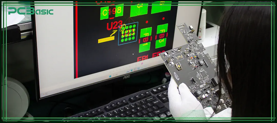
Visual inspection is a standard PCBA testing method involving visual examination of PCBs. The process checks for any defects, damages, or abnormalities that may have occurred during the manufacturing process. The equipment includes magnifying lenses or microscopes, which help inspect minute component sizes and placements. Good lighting is essential.
Visual inspection is usually the first test done and can find issues like broken or misplaced components, cold solder joints, incorrect component values/types, and conformal coating flaws.
Advantages:
● Simple
● Non-intrusive
● Catches gross defects
Disadvantages:
● Subjective
● Some issues require extra equipment.
Precaution: Ensure adequate lighting and magnification levels for visual inspection.
2. PCBA SMT First Article Inspection
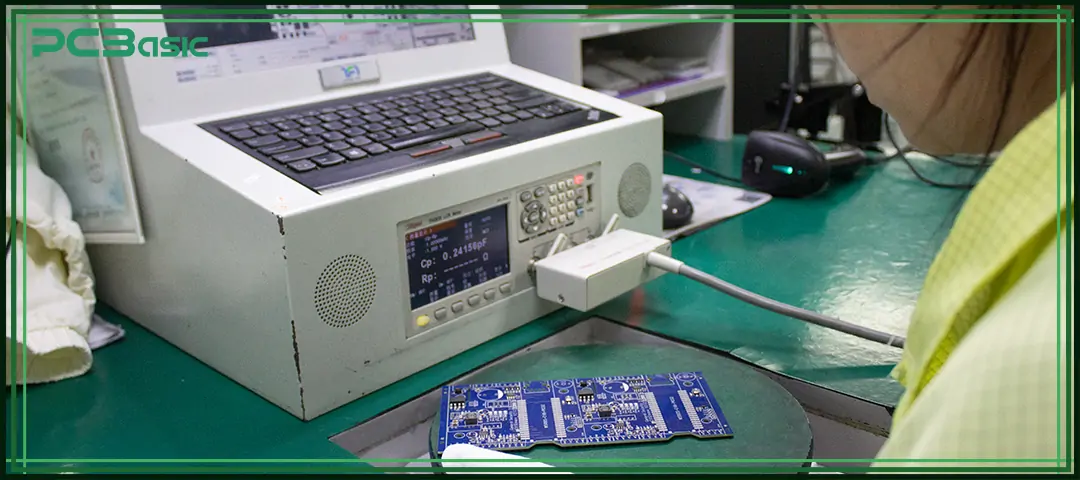
PCBA SMT First Article Inspection is a thorough verification of Printed Circuit Board Assemblies (PCBAs) at the beginning of a new production run. It ensures all design and component placement specifications are met before full production.
Key pieces of equipment include automated optical inspection (AOI) machines, x-ray machines, and functional test systems. AOI uses cameras to compare the actual board against its design files, while X-ray detects any deficiencies invisible to the naked eye.
Advantages:
● Ensures the fixing of errors before mass production
● Identifies any design issues upfront
● Provides a baseline for quality checks on the subsequent production run
Disadvantages:
● Time-consuming process delays the start of mass production
● Requires shutdown of the production line for inspection
Precaution: Manufacturing the first article samples should utilize all planned production materials, processes, and equipment for the most accurate results.
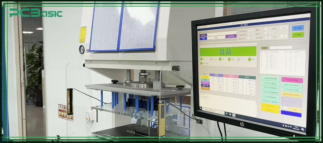
In-circuit testing (ICT) evaluates printed circuit boards (PCBs) by testing components and connections while still installed on the board. Using automated test equipment (ATE), ICT sends test signals into the circuit board and analyzes responses to verify that components, connections, and basic functionality match the design.
Advantages:
● Tests complete circuit without removing components
● Tests components interactively in their operating environment
● Faster than testing components individually
Disadvantages:
● Only tests for basic faults and may miss more complex issues
● Test fixtures and ATE equipment require investment
Precaution: Take caution not to damage circuit paths during test probe connection and disconnection.
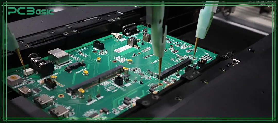
Flying probe testing is a quick and reliable way to test printed circuit board assemblies (PCBAs) and printed circuit boards (PCBs). It uses a computer-controlled probe card with multiple fine needle probes that 'fly' over the board surface to contact circuit traces and test points.
The probes are attached to automated positioners that precisely move them into contact with designated test points. This allows the flying probe tester to check multiple circuit paths and components simultaneously for defects such as short circuits, opens, and incorrect resistance values.
Advantages:
● High testing speed as it checks multiple points simultaneously
● Very high accuracy due to computer-controlled probe positioning
● Finds a variety of defects, including intermittent faults
Disadvantages:
● Requires specialized equipment and software, which can be expensive to purchase and maintain
● You can only access test points; buried components require other methods
Precaution: Be careful when handling the fine probe tips to avoid causing any damage during testing.
5. Automated Optical Inspection (AOI)
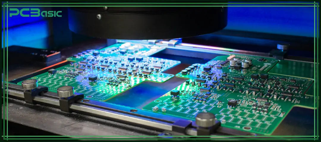
Automated Optical Inspection (AOI) is an important PCBA testing method that utilizes automated cameras and machine vision software to capture images and detect defects on printed circuit boards. The AOI system scans the PCBA with cameras from different angles as it goes through the inspection machine.
The captured images are then analyzed against a reference image using image processing algorithms to check for defects like missing, misplaced, or incorrectly oriented components. AOI systems allow for fast, accurate, and repeatable inspection of PCBA assemblies and are commonly used in manufacturing industries to ensure quality.
Advantages:
● Highly accurate and repeatable results
● Can inspect the entire board area quickly
● Finds even minute defects invisible to the human eye
● Reduces the need for manual visual inspection
Disadvantages
● Requires high-resolution cameras and machine vision software
● Component shadows or glare can hamper detection
Precaution: Proper lighting setup is critical for defect-free image capture.
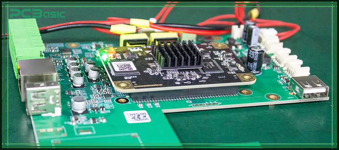
Burn-in testing is a reliability testing method where PCBAs undergo operation for an extended time. It is usually done at their maximum rated temperature, voltage, and frequency.
The testing process stresses the components and weeds out assembly and component failures that occur early in a product's life. Burn-in is done in temperature chambers or ovens where PCBAs are continuously operated for up to 200 hours.
Advantages:
● Potential early-life failures are identified before field deployment
● Components are exercised at maximum conditions
● Accelerates detection of design or manufacturing flaws
Disadvantages:
● Time-consuming process that increases testing costs
● Elevated temperatures may damage components that would otherwise function properly
Precaution: Burn-in should be done carefully to monitor component temperature and avoid overheating issues.
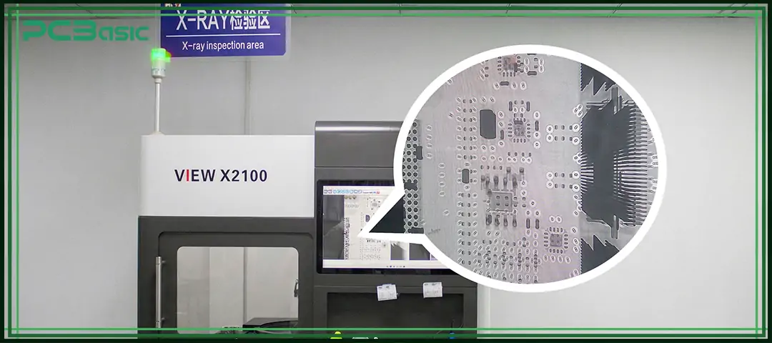
X-ray inspection is a non-destructive testing method to evaluate printed circuit board assemblies' internal structure and composition. It works on the principle of bombarding PCBs with X-rays and analyzing the resulting pattern of beams after they pass through the material.
The main equipment used is an X-ray generator, which produces X-rays, and an X-ray detector to record the patterns. It is commonly used to check for defects like incorrect placement, missing or poorly soldered components, and voids or gaps in solder joints.
Advantages:
● Precisely detects internal faults and defects impossible to observe otherwise
● Provides an inspection of the entire board quickly
● Can inspect boards in a populated state
Disadvantages:
● Requires expensive equipment and maintenance
● PCBs need to be moved through the scanner, limiting throughput
Precaution: Be careful to protect yourself against X-ray radiation exposure during the operation.
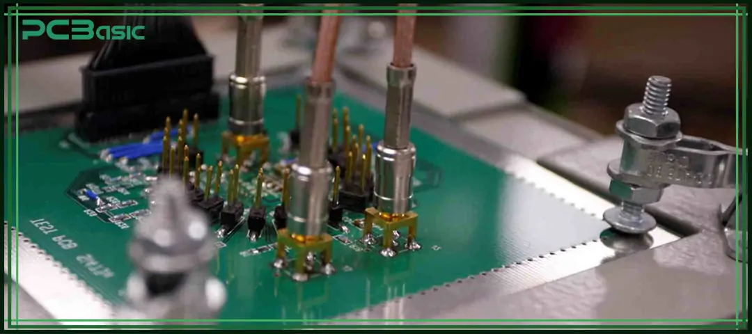
Fatigue testing subjects PCBAs to repeated loading and unloading to determine the product's reliability over time. The PCBA is secured in a test rig or fixture, and a force is repeatedly applied via an actuator at set intervals.
This tests the components and solder joints for potential failures from repeated mechanical stresses resembling long-term usage.
Advantages:
● Tests the durability and long-term reliability of solder joints and components
● Identifies potential weak points before full-scale production
● Accelerates the effects of long-term usage
Disadvantages:
● Time-consuming testing process
● Requires specialized fatigue testing equipment
Precaution: Components must be securely fastened during high-cycle fatigue testing to avoid detachment.
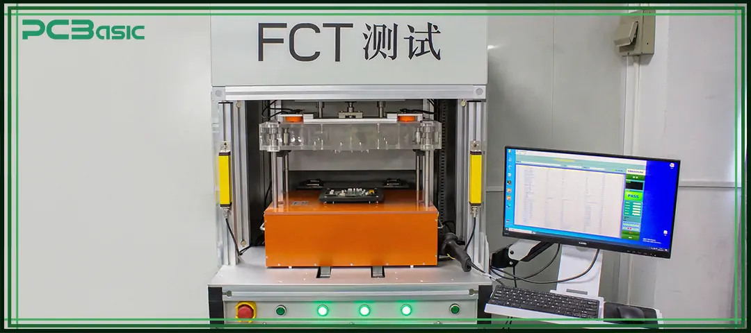
Functional testing is used to validate whether a PCBA is functioning per its design specification. In this method, test signals are given as input to the PCBA, and corresponding output signals are analyzed to check if components are working individually and as an integrated system.
The testing process involves the use of specialized functional test equipment like signal generators, oscilloscopes, and logic analyzers to apply input waveforms and monitor output responses.
Advantages:
● Checks the complete functionality of the PCBA
● Tests actual performance under rated conditions
● Ensures reliability of the design
Disadvantages:
● Time-consuming as it tests the full operation
● Requires specialized functional test equipment
Precaution: All safety protocols must be followed while handling live circuitry during functional testing.
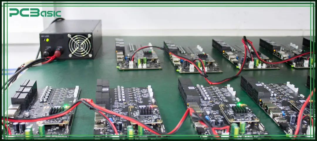
The aging test subjects PCBAs to extreme environmental conditions, such as high temperature and humidity, for a period of time. This allows manufacturers to check if components can withstand hazardous environmental stresses over prolonged usage.
The test is conducted by placing PCBAs inside climate chambers, which control and monitor temperature and humidity levels. Some key applications of the aging test include evaluating the long-term reliability of components and checking the sustainability of PCBAs against harsh working environments.
Advantages:
● Accelerates discovery of potential defects and failures
● Simulates real-world usage conditions
● Ensures long operational life under stressful conditions
Disadvantages:
● Time-consuming process
● Requires specialized, expensive chamber equipment
Precaution: Be careful to prevent physical damage to PCBAs during transfer in and out of climate chambers.
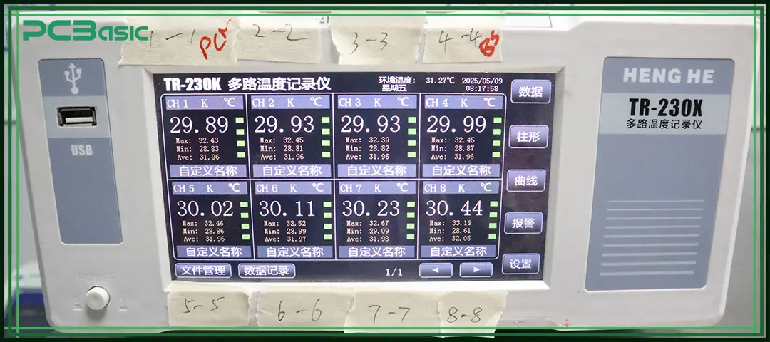
The Hash Environment tests the components on PCB assemblies under high temperature and humidity conditions to check their reliability and functional integrity. In this test, the assemblies are placed in a climatic chamber, which is maintained at elevated temperature (around 85°C) and high relative humidity (85% RH) to simulate harsh environmental conditions.
The equipment used is a programmable climatic chamber that can accurately control and monitor temperature and humidity as per IEC standard testing protocols.
Advantages:
● Tests long-term reliability of components under extreme conditions
● Finds weaknesses in materials and workmanship
● Certifies components to work in hazardous environmental zones
Disadvantages:
● It is a lengthy testing process
● Climate chambers require large floor areas and high energy costs
Precaution: You must be careful to avoid moisture condensation during transfer in and out of the climatic chamber.
12. Manufacturing Defect Analysis Test
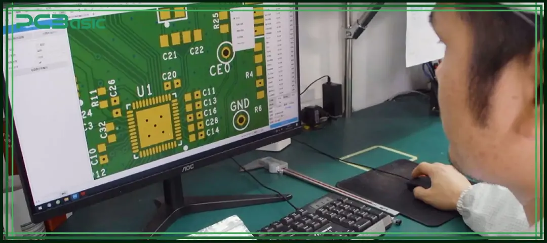
The Manufacturing Defect Analysis Test helps identify potential defects introduced during the assembly process of PCBAs. This non-destructive test uses high-resolution X-ray imaging to examine a PCB's internal structure and components.
Any discrepancies in component placement, solder bridges, cold solder joints, and missing or misplaced components can be easily detected. The X-ray equipment typically used has high-energy capabilities to penetrate through board materials without damaging the assembly.
Advantages:
● Precisely locates potential defects challenging to find via visual inspection
● Does not require disassembly of the PCBA for testing
● Provides a permanent video record for traceability
Disadvantages:
● High cost of equipment and maintenance
● Exposure to X-ray radiation requires strict safety compliance
Precaution: The test should only be performed by trained professionals licensed to operate X-ray equipment and following all radiation safety procedures.
Testing PCBAs often reveals the following common defects:
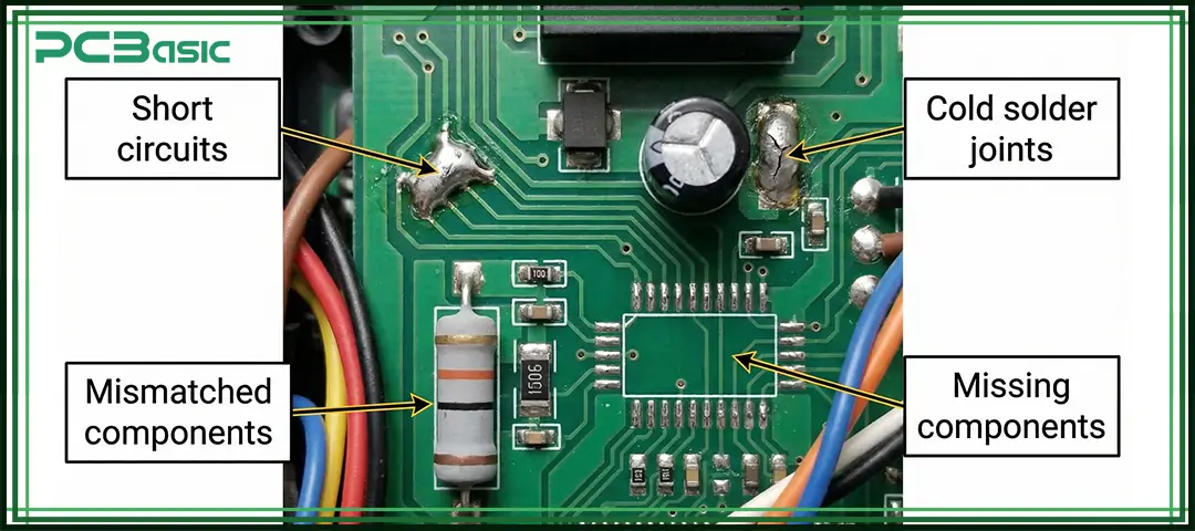
● Short circuits: When solder or stray metal connects components that should not be connected, it can cause boards to fail to power on or function incorrectly.
● Cold solder joints: Solder did not properly flow and bond between components and the board, resulting in weak connections that can fail over time.
● Mismatched components: The wrong resistor, capacitor, or integrated circuit may be installed due to incorrect part placement or mixing up similar-looking parts.
● Missing components: Components not properly inserted during assembly are regularly spotted, and testing ensures all required parts are present for the board to function as designed.
Addressing these typical defects is important for producing high-quality PCBAs that will reliably perform as intended. Testing catches these issues to improve product quality and reliability.
PCBA testing is not a single action, but a systematic process composed of multiple inspection and verification methods. A well-designed testing process can detect defects early, improve the yield rate, and ensure the reliability of the product. The following are the commonly used standard testing steps in PCBA manufacturing:
Before starting the test, the tester should complete a series of preparations, including reviewing the Gerber files, BOM lists and test point design, confirming whether there is a proper Design for Testability (DFT, such as test pads and test points), preparing test fixtures (for ICT/FCT) and testing programs, and confirming that the testing equipment has been calibrated
PCBA testing usually starts with the basic but crucial step. PCBA visual inspection mainly includes checking whether component placement, polarity, and orientation are correct, observing obvious defects such as missing components, solder bridges, and tombstoning, and at the same time using a microscope or magnifier to inspect fine-pitch components.
Visual inspection can quickly eliminate obvious assembly errors.
Automated Optical Inspection (AOI) is used for high-speed detection to ensure that the soldering quality meets standards. The main checks include identifying cold joints, insufficient or excessive solder, as well as voids or cracks.
For hidden solder joints, such as BGA and QFN, X-Ray inspection is used
Electrical testing is used to verify the circuit connection and basic functionality, including:
• Continuity Test: Check for open circuits or short circuits and confirm that all circuit net connections are correct.
• In-Circuit Test (ICT): Measure parameters such as resistance, capacitance, and voltage, verify the values and polarity of components, and detect component-level defects during the manufacturing process
• Flying Probe Test (for prototypes/small batches): It enables rapid testing without fixtures, is flexible and suitable for low-volume production
Functional testing simulates the real operating condition of the PCBA, used to ensure the entire board works properly as a system.
The board is powered on, input signals are applied, and output responses are analyzed, which is used to verify the signal processing function of the PCBA, communication interfaces (such as UART, USB, etc.) and the operating status of the software/firmware
In PCBA involving smart or embedded systems, programming and calibration are required to ensure that the equipment can operate normally and meet the design requirements:
• Firmware Programming: Load application code or bootloader
• Parameter Calibration: Adjust sensors, voltage references, or RF parameters
• Configuration Writing: Initialize and store data in EEPROM or Flash
Verify the performance of the product in long-term and extreme environments, including
• Burn-in Test: Continuous operation at high temperature
• Thermal Cycling Test: Repeated heating and cooling cycles
• High Temperature & Humidity Test (85°C / 85% RH): Environmental resistance
• Vibration Test: Mechanical stability
The final quality check before shipment requires a final visual inspection of the PCBA, sampling or full functional testing, and generating test reports and traceability data (via MES systems).
PCBA testing is a multi-layered and multi-stage systematic project, from appearance inspection to functional verification, and then to environmental reliability testing; each step is critical. By establishing a scientific testing process, manufacturers can effectively reduce defect rates, enhance product reliability, and ensure that products meet industry standards before being delivered to customers.
PCBA testing has come a long way from simply testing circuit continuity with multimeters. Advances in automated testing equipment and software have allowed manufacturers to test boards for issues during production thoroughly. As electronics continue to become more integrated and complex, PCBA tests will also need to evolve to maintain quality standards.
If your business needs robust, high-quality PCBA production, consider partnering with an industry leader like PCBasic. Our full-service manufacturing includes cutting-edge PCBA testing that can give you peace of mind and improve your product quality. Contact us today to discuss how they can help meet your testing needs.
Looking for a PCB or PCBA quote? Contact us now: JS@pcbasic.com.

Assembly Enquiry
Instant Quote
Phone contact

+86-755-27218592
In addition, we've prepared a Help Center. We recommend checking it before reaching out, as your question and its answer may already be clearly explained there.
Wechat Support

In addition, we've prepared a Help Center. We recommend checking it before reaching out, as your question and its answer may already be clearly explained there.
WhatsApp Support

In addition, we've prepared a Help Center. We recommend checking it before reaching out, as your question and its answer may already be clearly explained there.