Global high-mix volume high-speed PCBA manufacturer
9:00 -18:00, Mon. - Fri. (GMT+8)
9:00 -12:00, Sat. (GMT+8)
(Except Chinese public holidays)
Global high-mix volume high-speed PCBA manufacturer
9:00 -18:00, Mon. - Fri. (GMT+8)
9:00 -12:00, Sat. (GMT+8)
(Except Chinese public holidays)
HomePage > Blog > Knowledge Base > What Is a FET (Field-Effect Transistor)?

The field-effect transistor (FET) ranks among the most revolutionary state-of-the-art developments in modern electronics. The FET works quite differently from its predecessor, the bipolar junction transistor (BJT), which makes it particularly valuable in modern electronic design. A field-effect transistor is a three-terminal semiconductor device that uses an electric field to control current flow. The name "field-effect" points to its vital operating principle - voltage applied to one terminal (the gate) creates an electrical field that controls current flow between the other two terminals (source and drain).
Several key differences set FETs apart from bipolar junction transistors. FETs are voltage-controlled devices, not current-controlled like BJTs. This means they need minimal input current and offer very high input impedance - a huge advantage in many circuit designs. On top of that, FETs work with only majority carriers (either electrons or holes). This makes them unipolar devices, unlike BJTs that use both carrier types.
The simple structure of a FET has three main terminals:
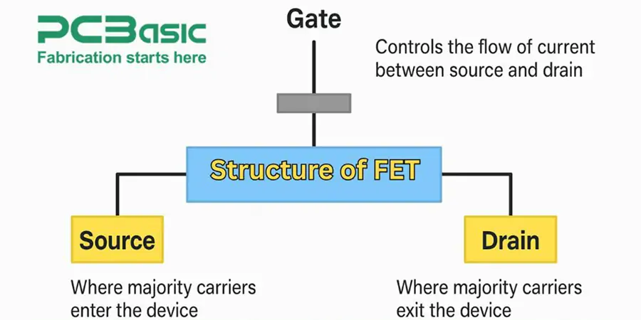
The gate terminal's voltage creates an electric field that enhances or depletes the conductive channel between source and drain. This controls current flow and lets FETs serve as very efficient switches or amplifiers.
FETs come in different varieties. The two most common types are Junction Field-Effect Transistors (JFETs) and Metal-Oxide-Semiconductor Field-Effect Transistors (MOSFETs). JFETs usually operate in depletion mode (normally on), while MOSFETs can work in either enhancement mode (normally off) or depletion mode.
Engineers classify FETs as either N-channel or P-channel types, based on whether electrons or holes act as majority carriers. This classification determines their operational characteristics and where they work best.
FETs have become irreplaceable in modern electronics. Their high input impedance, low power usage, and compatibility with integrated circuit manufacturing make them vital components in almost every electronic device. These versatile components power everything from computer microprocessors to electric vehicle management systems. FETs do have their limitations. They can be sensitive to static electricity, and circuit implementation requires specific design considerations.
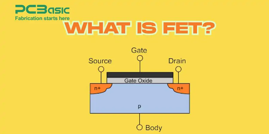
Field-effect transistors (FETs) are among the most important semiconductor devices that power modern electronics. These three-terminal components have a unique way of controlling electric current flow that makes them highly effective.
A transistor is a semiconductor device that amplifies or switches electronic signals. These devices are the lifeblood of modern electronics and serve as simple building blocks in integrated circuits. Transistors come in three main types: bipolar junction transistors (BJTs), field-effect transistors (FETs), and insulated-gate bipolar transistors (IGBTs). Over the last several years, transistors have made electronic devices smaller and helped develop the advanced technologies we use today.
The term "field-effect" explains how these devices work at their core. An electric field in a field-effect transistor controls current flow through a semiconductor channel. The process starts when the voltage reaches the gate terminal. This creates an electric field across an insulating layer and forms a depletion region in the channel. The region changes the number of free charge carriers available, which adjusts the channel's conductivity. FETs are highly efficient because they can control current precisely without needing much input current.
While both devices do similar things, FETs and BJTs work quite differently:
|
Feature |
FET (Field Effect Transistor) |
BJT (Bipolar Junction Transistor) |
|
Control Mechanism |
Voltage-controlled (requires voltage) |
Current-controlled (requires base current) |
|
Charge Carriers |
Uses one type (either electrons or holes) |
Uses both electrons and holes |
|
Input Impedance |
Very high (millions of ohms) |
Lower (thousands of ohms) |
|
Power Consumption |
Low (due to voltage control) |
Higher (due to current control) |
|
Switching Speed |
Faster switching, suitable for high-frequency use |
Slower switching compared to FETs |
|
Noise Level |
Lower noise (no junctions in conduction path) |
Higher noise (due to junctions) |
FETs have reshaped the scene of electronics with their efficiency, compact size, and ability to work well in integrated circuits. Their high input impedance and low power needs make them perfect to use when you need minimal loading and power efficiency.
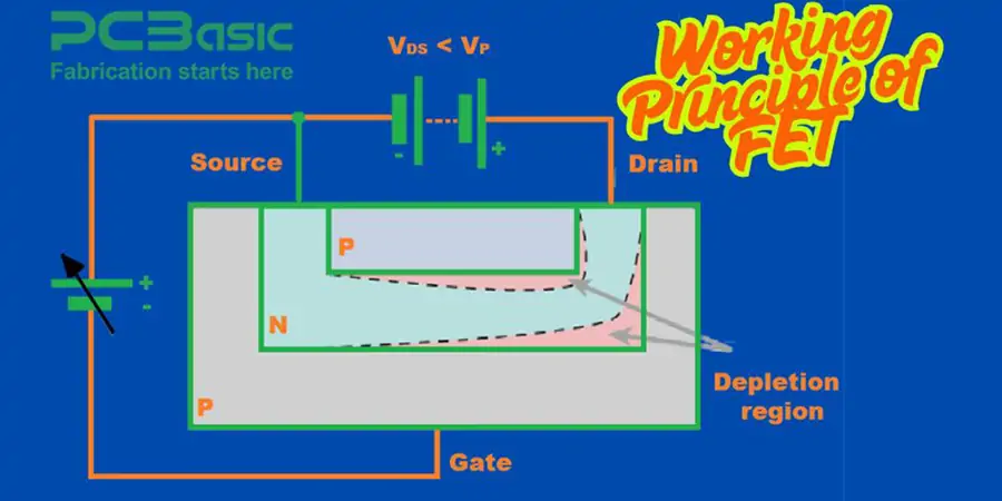
The physical components and electrical behavior of field-effect transistors reveal how they work. FETs have an elegant design that lets us control current through semiconductor material with great precision. These devices are the lifeblood of modern electronics.
FETs have three main terminals that work together to control electrical current:
● Source: Acts as the origin of the majority carriers (electrons in N-channel or holes in P-channel devices)
● Drain: Serves as the destination for these carriers, creating the current path
● Gate: Functions as the control terminal that regulates current flow between the source and the drain
Different FET types arrange these terminals in various ways, but their basic roles stay the same. The source usually serves as the reference point to measure voltage.
The sort of thing I love about field-effect transistors is their ability to control current flow without direct electrical contact. A voltage applied to the gate terminal creates an electric field that goes through the semiconductor material. This field attracts or repels charge carriers in the channel region and changes its conductivity.
To cite an instance, an N-channel enhancement-mode MOSFET needs a positive gate voltage to attract electrons and form a conductive channel. Higher voltage improves conductivity, while lower voltage limits current flow.
FETs need a conductive path called the "channel" between source and drain. This channel comes in two basic types:
N-channel: Uses electrons as majority carriers. Positive gate voltage improves conductivity in enhancement-mode devices or reduces it in depletion-mode types.
P-channel: Uses holes as majority carriers. Negative gate voltage controls channel conductivity, working opposite to N-channel devices.
N-channel FETs conduct current from drain to source with a positive gate voltage (compared to source). P-channel FETs work the opposite way - they conduct with a negative gate voltage. This opposite behavior gives designers complementary options for circuits.
Gate control logic follows a simple pattern. N-channel devices turn on with a positive gate voltage. P-channel types activate with a negative gate voltage. This complementary behavior forms the foundations for efficient CMOS (Complementary Metal-Oxide-Semiconductor) technology in most integrated circuits.
The biggest difference in FETs is their voltage-controlled nature. BJTs need a constant base current to conduct, but FETs only need a gate voltage to keep working. This is a big deal as it means that input impedance often exceeds 10^9 ohms. FETs make ideal input stages for amplifiers and applications that need minimal loading.
FETs also use very little power because their voltage control system draws almost no gate current during normal operation.
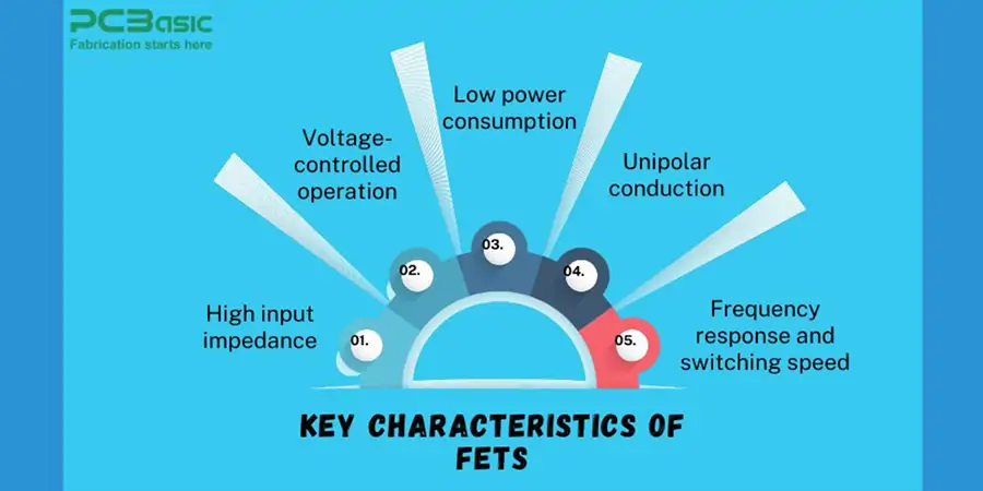
Field-effect transistors have unique properties that make them vital to modern electronics. These properties define how well they work in different applications and give them clear advantages over other semiconductor devices.
FETs showcase input impedance that reaches thousands of megaohms at low frequencies. The reverse-bias gate junction creates this property by acting like an open circuit. This lets FETs sample signals without interfering with the signal source. Real-world applications see input impedance values from hundreds to thousands of megaohms. These values make FETs perfect for circuits that need minimal interaction.
FETs differ from bipolar junction transistors because they work as voltage-controlled devices. The gate terminal's voltage controls the output current. The gate needs just enough current to charge its capacitance. An electric field forms when a voltage hits the gate. This field changes the channel's conductivity between the source and the drain. The result is current flow modulation without power-hungry input current.
The minimal power needs of FETs make them great for battery-powered devices. They need no extra power after gate charging or discharging. BJTs, however, need a constant base current. This efficiency means circuits can be smaller because they generate less heat. FETs now serve as core components in portable electronics' power management systems.
FETs stand apart from BJTs as unipolar devices. They use either electrons (n-channel) or holes (p-channel) as charge carriers. This basic difference shapes how they work and behave electrically. Their simple charge transport system helps them run efficiently with straightforward control logic.
FETs excel at switching speeds, which work great in digital circuits and high-frequency uses. They don't face the charge storage issues that stymie bipolar transistors. Higher frequencies mean smaller passive components but more switching losses. Circuit designers must balance this trade-off when they need both small size and high efficiency.
Field-effect transistors come in different types, each with its own operational characteristics. The semiconductor world features two dominant FET categories: Junction Field-Effect Transistors (JFETs) and Metal-Oxide-Semiconductor Field-Effect Transistors (MOSFETs).
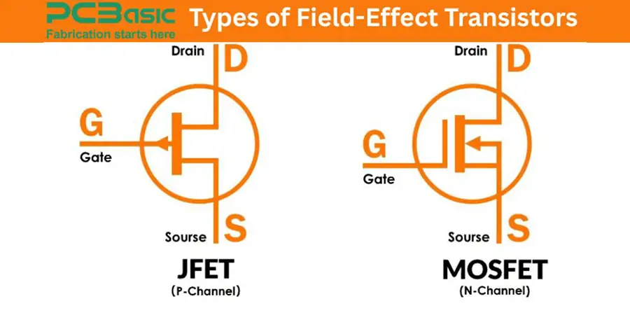
JFETs emerged as the first field-effect transistors and have a simpler structure than MOSFETs. These devices use a reverse-bias PN junction to control current flow through a semiconductor channel. JFETs differ from MOSFETs mainly in their gate construction - they use a direct semiconductor junction at the gate instead of an insulated metal gate.
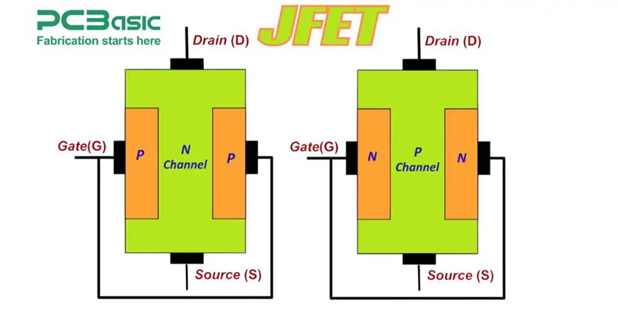
● Basic concept and construction
A JFET's core structure consists of a semiconducting channel with two ohmic contacts (source and drain) and a gate region that forms a PN junction with the channel. N-channel JFETs use P-type semiconductor material to form the gate around an N-type channel. P-channel JFETs work the opposite way, with N-type gate material surrounding a P-type channel.
The JFET's channel creates a conductive path for majority carriers flowing from source to drain. Changes in gate voltage expand or contract the depletion region at the PN junction, which alters the channel width and controls current flow.
● Normally-on operation
JFETs work in depletion mode, making them "normally-on" devices. The channel stays conductive and allows maximum current flow when no voltage exists between gate and source (VGS = 0). A reverse bias applied to the gate-channel junction widens the depletion region and restricts current flow through the channel.
● Common analog usage
JFETs excel in analog circuits thanks to their unique properties:
● Low-noise amplifiers: Their natural low-noise characteristics make them perfect for front-end amplification in sensitive equipment
● Voltage-controlled resistors: This variable resistance feature works well in audio equipment and signal processing
● Constant current sources: The high output impedance helps create stable current references
● Switch applications: They offer excellent linearity for certain switching needs, though they're slower than MOSFETs
JFETs shine in instrumentation and audio applications where signal integrity matters most, thanks to their high input impedance and good linearity.
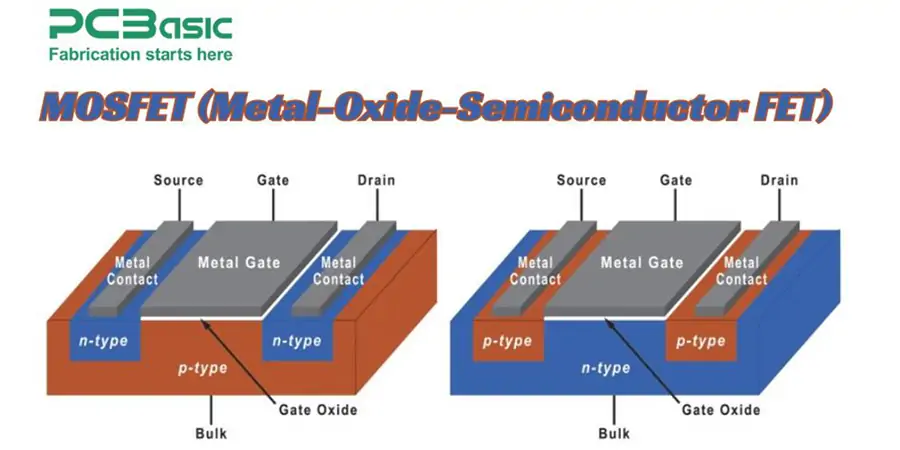
MOSFETs are the foundations of modern electronics and dominate today's semiconductor industry through their versatile characteristics and applications. These devices differ from JFETs because they have an insulated gate structure where a thin oxide layer keeps the gate separate from the channel to prevent gate current flow.
● Enhancement-mode vs depletion-mode
Enhancement-mode MOSFETs work as "normally-off" devices that need a gate voltage to create a conductive channel. These devices won't allow current flow between the drain and source without gate-source voltage. Depletion-mode MOSFETs take a different approach and function as "normally-on" devices that conduct at zero gate voltage. This creates distinct switching behaviors - enhancement mode needs voltage to turn on, while depletion mode requires opposite polarity voltage to turn off.
● N-MOS vs P-MOS
N-channel MOSFETs (NMOS) utilize electrons as majority carriers and have N-type source/drain regions on a P-type substrate. These devices become active with a positive gate voltage that attracts electrons to form a conductive channel. P-channel MOSFETs (PMOS) work differently by using holes as carriers and feature P-type source/drain regions on an N-type substrate. PMOS devices need a negative gate voltage relative to the source.
Key differences include:
● NMOS switches faster because of higher electron mobility
● PMOS uses less power when "on"
● NMOS needs less space for equivalent current capacity
● PMOS shows better noise immunity
● Widely used in switching, microcontrollers, power management
MOSFETs shine in many applications thanks to their fast switching capabilities and high input impedance. These devices serve as essential components in digital circuits, from microprocessors to memory chips. MOSFETs control electrical flow efficiently in DC-to-DC converters. Their thermal stability ensures reliable operation across various temperature ranges.
● Advantages of JFET
JFETs offer unique benefits in specific applications despite MOSFETs' popularity:
● Better protection against static electricity damage
● Higher linearity for sensitive analog applications
● Less complex manufacturing process
● Enhanced performance in certain high-frequency applications
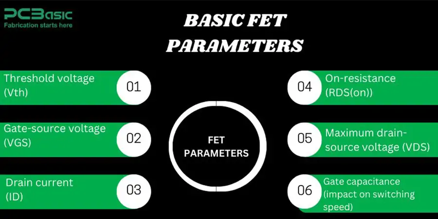
Designers working with field-effect transistors need to understand several key electrical parameters that define their behavior. These basic specifications show how an FET will work in different circuits and applications.
A FET's threshold voltage is the minimum gate-source voltage that creates a conductive channel between the drain and the source. This parameter tells you when enhancement-mode MOSFETs start to turn on. Most common devices have Vth values between 0.5V and 4V, which marks the boundary between cut-off and active regions. The parameter changes with temperature and usually drops as things heat up.
The gate-source voltage controls how well the FET's channel conducts. N-channel enhancement MOSFETs need VGS above Vth to let current flow, while P-channel types work with VGS below their negative threshold. Data sheets list maximum VGS limits (usually ±20V) to protect the gate oxide. They also specify minimum VGS values to ensure the device turns on fully in switching applications.
The drain current shows how much current flows from the drain to the source. VGS controls ID in the active region until it levels off in saturation. Package type and cooling determine the maximum continuous ID ratings, and power FETs can handle hundreds of amperes. Pulsed ID ratings are a big deal as it means they can go higher than continuous ratings.
RDS(on) measures the resistance between the drain and source when the FET turns on fully. This value affects power loss through P = ID²×RDS(on). Today's power MOSFETs are super-efficient switches with values under 1mΩ in some cases. Temperature makes RDS(on) go up, so you need to account for this in hot environments.
VDS ratings tell you the highest voltage the FET can handle between the drain and source before breaking down. Going over this limit can destroy the device. Power MOSFETs come with VDS ratings from 30V to 1500V based on what you need them for.
Gate capacitance controls how fast the FET can switch. A higher capacitance means the device needs more time to charge and discharge, which limits switching speed. The total gate charge (Qg) spec gives you a better picture of switching energy needs, especially in power circuits where quick switching helps reduce losses.
FETs are the lifeblood of modern electronic design because of their unique advantages. These devices are a great way to get benefits in applications of all sizes, from tiny mobile devices to complex power systems.
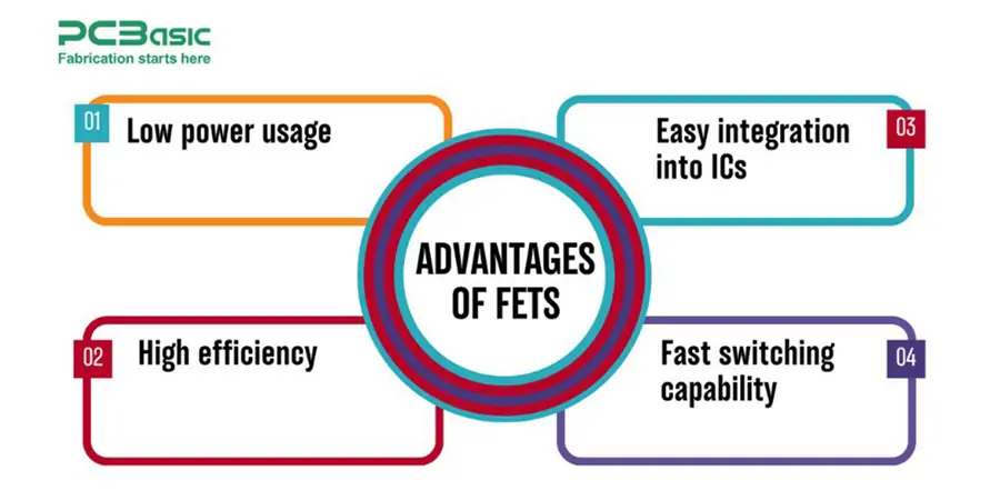
● Low power usage
Field-effect transistors need minimal power, which makes them perfect for battery-powered devices. The gate needs power only during charging or discharging. This stands in stark contrast to bipolar junction transistors that need a constant base current to maintain conduction. FETs allow greater miniaturization because they need less heat dissipation. Some thermal FETs consume as little as 1μA in LED applications, which prevents lights from glowing faintly when turned off.
● High efficiency
FETs offer more than simple power savings. GaN FETs shine with their remarkable efficiency due to low series resistance, faster switching times, and lower reverse recovery charge. This reduces conduction, switching, and reverse recovery losses. Modern power MOSFETs can achieve on-resistance values under 1mΩ, which leads to minimal power loss even with high currents.
● Easy integration into ICs
Field-effect transistors blend perfectly into modern semiconductor processes. The MOSFET's planar structure made it the first compact transistor suitable for miniaturization and mass production. The US Patent and Trademark Office recognizes them as a "groundbreaking invention that revolutionized life and culture around the world". FETs also work with existing silicon CMOS production facilities, making them budget-friendly.
● Fast switching capability
FETs deliver impressive performance with switching speeds of 10-11 nanoseconds in high-frequency applications. These quick transitions lead to better signal control and improved passive filter designs with higher cutoff frequencies. The practical benefit shows in reduced ripple currents that allow smaller inductors, capacitors, and transformers, reducing system size and weight. Power MOSFETs now focus on low gate charge and switching speed, which is vital for high-efficiency power conversion.
Field-effect transistors offer many benefits, but they also have some limitations that designers need to address. Let's look at the drawbacks you should think about when picking components for electronic applications.
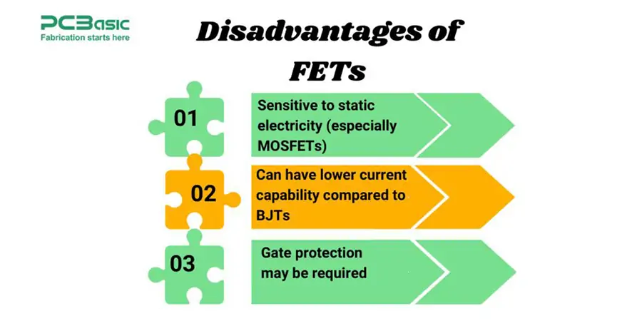
● Sensitive to static electricity (especially MOSFETs)
The very high input impedance that makes FETs so valuable also makes them easy targets for electrostatic discharge (ESD). This weakness comes from the very thin gate oxide layer, which can be just 5 atoms thick. Static electricity can permanently damage this delicate gate oxide during handling or when mounting the board.
The damage happens when gate-to-source voltage goes past the breakdown threshold and burns a tiny hole in the gate dielectric. This creates either a low resistance or a zener effect between gate and source with less than ±20 volts applied. These devices can be destroyed permanently with just a quick exposure to electrostatic discharge.
● Can have lower current capability compared to BJTs (depending on design)
FETs don't handle current as well as bipolar junction transistors in some applications. High-power MOSFETs typically work as high-current but low-voltage devices. BJTs do better with low-frequency, high-current applications.
FETs also show lower transconductance than BJTs of similar size. This makes them less ideal for certain amplifier applications, especially when you need high gain or work with weak input signals.
● Gate protection may be required
FETs need extra protection circuits because they're sensitive to overvoltage. A common fix is to put an ESD protection component between the gate and source terminals. Some protection methods you can use:
● Zener diodes between gate and source to clamp high voltages
● Series resistors that limit input current when protection diodes conduct
● Special ESD protection diodes made for FET applications
Good handling procedures are vital beyond component-level protection. This means grounding equipment, wearing anti-static clothes, and using conductive packaging materials to store and move components. These safety measures help prevent damage from static charges that could make these sensitive devices stop working.
Field-effect transistors power countless devices and serve as essential components in modern technological systems. Their unique electrical properties make them ideal for applications that range from tiny consumer gadgets to massive industrial equipment.
FETs are the backbone of smartphone processors, memory chips, and power management systems in consumer electronics. The CMOS process technology employs complementary pairs of p-channel and n-channel MOSFETs that are the foundations of digital integrated circuits. These devices enable our digital lifestyle through vibration modes in wearables and battery management in laptops.
The automotive sector demonstrates FETs' versatility. Electric vehicle drive systems use IGBTs to control motor speed and torque. The 600-V CoolMOS S7TA super-junction MOSFET gives 40% higher accuracy than standalone sensors through its integrated temperature sensor, specifically designed for automotive applications. These breakthroughs enhance vehicle range, acceleration, and safety with precise electrical control.
Industrial systems make use of FETs for motor drives and power conversion. IGBTs have become the preferred choice for industrial motor drives that enable precise speed regulation in manufacturing equipment. MOSFETs play vital roles in variable frequency drives and convert electrical energy efficiently through high-frequency switching.
FETs excel in specialized roles:
● High-input impedance amplifiers for oscilloscopes and electronic measurement equipment
● RF amplifiers in FM tuners and communication systems, valued for their low noise levels
● Voltage-controlled resistors in operational amplifiers and tone controllers
● Mixer circuits in receivers, where low intermodulation distortion improves signal quality
Power FETs have evolved significantly. Some vertical DMOS types feature operating voltages up to 650V, current ratings to 16A, and switching speeds approaching 2GHz. "Smart" MOSFETs now include built-in protection against damage from short circuits, over-temperature conditions, and electrostatic discharge.
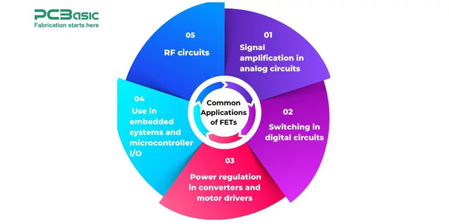
● Signal amplification in analog circuits
Field-effect transistors (FETs) are integral components in analog circuit design due to their high input impedance and low noise characteristics. These features make FETs ideal for signal amplification in applications such as audio preamplifiers, operational amplifiers, and sensor interfacing. Junction FETs (JFETs) are particularly favored in low-noise amplifier designs, including those used in audio and RF systems, where preserving signal integrity is crucial.
● Switching in digital circuits (logic gates, memory)
In digital electronics, FETs, especially Metal-Oxide-Semiconductor FETs (MOSFETs), serve as the fundamental building blocks of logic gates and memory elements. Their fast switching speeds, low power consumption, and scalability make them suitable for constructing integrated circuits (ICs), including microprocessors and memory modules. In these applications, FETs operate as binary switches, toggling between cutoff and saturation regions to represent digital logic states.
● Power regulation in converters and motor drivers
Power FETs are widely used in circuits that require efficient energy management and control. In power converters, such as DC-DC regulators and inverters, FETs act as high-speed switches to modulate voltage and current. Similarly, in motor drivers, FETs enable precise control of motor operation through pulse-width modulation (PWM). Their ability to handle high currents and voltages makes them indispensable in power electronics.
● Use in embedded systems and microcontroller I/O
FETs are commonly found in embedded systems, often integrated into microcontroller input/output (I/O) structures. They are used to interface digital signals with external peripherals, drive LEDs, manage power gating, and switch loads. The low gate current requirement of FETs makes them ideal for microcontroller-based applications, where power efficiency is often a priority.
● RF circuits (JFETs in particular)
FETs, particularly JFETs and MESFETs, are employed in radio frequency (RF) circuits for their low noise figures and high-frequency response. Applications include RF amplifiers, oscillators, and mixers in communication systems. Their inherent properties enable effective handling of small signal variations at high frequencies, ensuring signal clarity and system performance in RF domains.
FET, especially JFETs and Mosfets, work in Radio Frequency (RF) circuit for their low noise numbers and high existing response. Applications include communication systems, RF amplifiers, mixers. Their underlying properties enable effective handling of small signal variations at high frequencies, ensuring clarity and system performance in RF domains.
Field-effect transistors represent a success in semiconductor technology that has reshaped electronic design. These devices light with voltage-controlled operations, low power requirements, and rapid replacement functions. The unique features of FETs make them important in many applications. Their high input impedance and strength efficiency stand out. JFETs provides better linearity in analog circuits, while MOSFETs manage digital electronics because of their production benefit and switching performance.
Today's electronic world is dependent on FET technology. You will find them everything from smartphones to electric vehicles. Their development extends what is possible in power management, switching speed and integration density. FETs act as important building blocks for technological progress, although stable sensitivity is still a challenge. Engineers and technicians can make a better option about components and circuit design by mastering these devices. New materials and structures promise better as the area grows, and opens opportunities for future applications.

Assembly Enquiry
Instant Quote
Phone contact

+86-755-27218592
In addition, we've prepared a Help Center. We recommend checking it before reaching out, as your question and its answer may already be clearly explained there.
Wechat Support

In addition, we've prepared a Help Center. We recommend checking it before reaching out, as your question and its answer may already be clearly explained there.
WhatsApp Support

In addition, we've prepared a Help Center. We recommend checking it before reaching out, as your question and its answer may already be clearly explained there.