Global high-mix volume high-speed PCBA manufacturer
9:00 -18:00, Mon. - Fri. (GMT+8)
9:00 -12:00, Sat. (GMT+8)
(Except Chinese public holidays)
Global high-mix volume high-speed PCBA manufacturer
9:00 -18:00, Mon. - Fri. (GMT+8)
9:00 -12:00, Sat. (GMT+8)
(Except Chinese public holidays)
HomePage > Blog > Knowledge Base > Copper Trace in PCBs: Everything You Need to Know
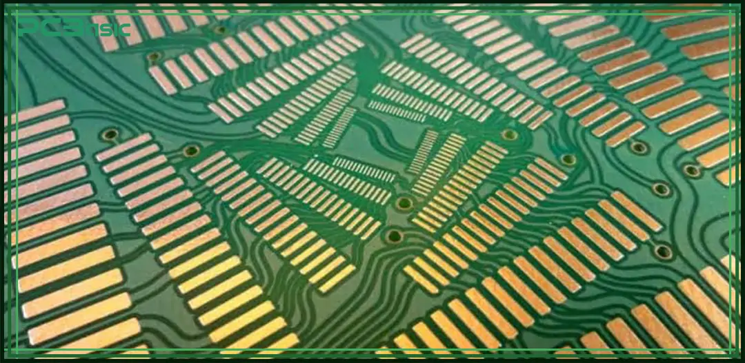
Take a close look at any printed circuit board. You’ll notice those thin, shiny lines weaving across the surface like a miniature roadmap. Those aren’t just there for show. They are copper traces. And they are absolutely critical to how your board functions.
Copper traces aren’t just shiny lines. They are the lifelines of your circuit. Every signal. Every bit of power. It all flows through them—from delicate ICs to power-hungry drivers.
But laying down a copper trace isn’t a guessing game. You can’t just draw a line and hope it holds up. Too thin? It overheats. Too wide? You waste space and possibly money.
That’s where engineering comes in. You need to size each trace based on current load, copper weight, and how much heat you can tolerate.
It's a trade-off. Width, thickness, temperature rise—all connected. Ignore one, and you risk failure. Get it right, and your board will run cooler, safer, and longer.
So, how do you get it right? That’s what we are diving into—how copper thickness, trace width, current, and temperature rise all connect in PCB design.

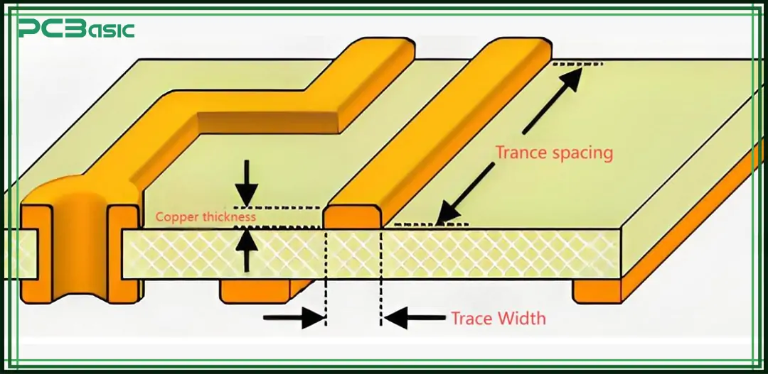
Not all copper is created equal at least not on a PCB. The thickness of your copper traces has a direct impact on how much current they can safely carry. Most standard boards use 1 oz copper, which measures about 1.4 mils (or 35 μm) in thickness. But once you start dealing with higher currents, that might not cut it. That's where heavier copper weights come in—2 oz, 3 oz, and even more, if needed.
So why does thickness matter? Simple. Thicker traces can carry more current without overheating. They also reduce resistance, which means better efficiency. But there's a trade-off. Thicker copper takes up more space and costs more. And in multi-layer PCBs, space is tight.
Here’s a general reference:
|
Copper Weight (oz/ft²) |
Thickness (mil) |
Thickness (μm) |
|
0.5 oz |
0.7 mil |
~18 µm |
|
1 oz |
1.4 mil |
~35 µm |
|
2 oz |
2.8 mil |
~70 µm |
|
3 oz |
4.2 mil |
~105 µm |
The takeaway? Copper thickness isn’t just a spec—it’s a performance lever. Use it wisely. And your board runs cooler and cleaner. Skimp on it, and you might end up with burned traces and failed prototypes.
Now, we are getting into real design work. One of the most critical tasks in PCB layout? Figuring out how wide each trace needs to be. It’s not just about fitting lines between pads. Each trace must carry current without overheating.
The goal is simple: choose a width that can handle the current load while keeping the temperature rise within safe limits. However, as you’ll see, the math behind it isn’t always so simple.
There are two main factors:
1. Current carrying capacity
2. Acceptable temperature rise
Trace width depends on both. The general rule is: Higher current = wider trace.
However, the actual number varies based on whether the trace is internal (inside the board) or external (on the surface) and how much temperature rise you can tolerate.
Here’s the equation, adapted from IPC-2221 (the old standard):
Width (mil) = (Current (A) / (K × ΔT^b))^(1/c)
Where:
• k = 0.048, b = 0.44, c = 0.725 for external layers
• ΔT is the temperature rise in Celsius
Sounds complex? You’re not alone. That’s why most engineers now rely on PCB trace width calculators that follow IPC-2152.

Instead of crunching numbers manually, most designers use an online trace calculator or PCB trace width calculator. These tools do all the hard math behind the scenes. You just plug in:
• Desired current
• Temperature rise
• Copper weight (in oz)
• Whether it’s internal or external
The tool tells you the minimum trace width you should use. Some calculators even allow you to adjust safety factors, voltage drop, and trace length.
Here are a few popular ones engineers trust:
• Advanced Circuits PCB Trace Width Calculator
• Saturn PCB Toolkit
• EEWeb Trace Width Calculator
Keep in mind, every trace width calculator is based on some form of IPC standard, usually IPC-2152, which replaced IPC-2221 for trace width vs current guidelines. IPC-2152 is more accurate. Because it considers real-world test data, including convection, trace spacing, and board material.
Whether you're designing a simple LED board or a complex power distribution PCB, a good PCB trace calculator helps save time and reduce design errors.

This is where things get interconnected. Let’s say you’re designing a PCB that handles 5 amps. You can achieve that in two ways:
1. Use a thicker copper layer and keep the trace narrow
2. Keep standard copper and make the trace much wider
Here’s a quick table (using IPC-2152 guidance):
|
Trace Width (inch) |
10°C 0.5oz |
10°C 1.0oz |
10°C 2.0oz |
20°C 0.5oz |
20°C 1.0oz |
20°C 2.0oz |
30°C 0.5oz |
30°C 1.0oz |
30°C 2.0oz |
|
0.01 |
0.5 |
1 |
1.4 |
0.6 |
1.2 |
1.6 |
0.7 |
1.5 |
2.2 |
|
0.015 |
0.7 |
1.2 |
1.6 |
0.8 |
1.3 |
2.4 |
1 |
1.6 |
3 |
|
0.02 |
0.7 |
1.3 |
2.1 |
1 |
1.7 |
3 |
1.2 |
2.4 |
3.6 |
|
0.025 |
0.9 |
1.7 |
2.5 |
1.2 |
2.2 |
3.3 |
1.5 |
2.8 |
4 |
|
0.03 |
1.1 |
1.9 |
3 |
1.4 |
2.5 |
4 |
1.7 |
3.2 |
5 |
|
0.05 |
1.5 |
2.6 |
4 |
2 |
3.6 |
6 |
2.6 |
4.4 |
7.3 |
|
0.075 |
2 |
3.5 |
5.7 |
2.8 |
4.5 |
7.8 |
3.5 |
6 |
10 |
|
0.1 |
2.6 |
4.2 |
6.9 |
3.5 |
6 |
9.9 |
4.3 |
7.5 |
12.5 |
|
0.2 |
4.2 |
7 |
11.5 |
6 |
10 |
11 |
7.5 |
13 |
20.5 |
|
0.25 |
5 |
8.3 |
12.3 |
7.2 |
12.3 |
20 |
9 |
15 |
24 |
So, yes, you can reduce trace width by increasing copper thickness. But again, there’s a balance between cost, space, and thermal performance.
This is why tools like the trace width calculator or trace thickness calculator are essential during the design phase. They let you play with parameters to find the most efficient design.
Let’s zoom in on something that often overlooks the actual size of the copper trace, meaning its cross-sectional area. That’s the trace width multiplied by the copper thickness.
Simple math, but it tells you a lot.
Area = Trace Width × Copper Thickness
The larger that area, the lower the resistance. And lower resistance means less heat gets generated when current flows through the trace.
But here’s the catch: current and temperature rise are directly linked. If you push more current through a trace without increasing its area, you're asking it to carry a heavier load than it was built for. Resistance turns that excess current into heat, and the temperature starts climbing fast.
So, what do you do? You either give the current more “room” by increasing the area—wider trace, thicker copper—or you reduce the amount of current you’re pushing through.
There’s no shortcut here. It’s all about balance. And remember, the trace’s location on the PCB also matters. External traces can cool off more easily, thanks to airflow. Internal traces? They’re trapped between layers and heat up quicker.
Here’s a quick comparison to put it into perspective:
2 oz copper, 150 mils wide trace:
Cross-sectional area = 150 mil × 2.8 mil = 420 mil²
Can safely carry ~6.5 A with a 20°C temperature rise
2 oz copper, 100 mils wide trace:
Cross-sectional area = 100 mil × 2.8 mil = 280 mil²
Heats up significantly faster under the same current
So, shaving a bit off the width might look harmless, but it has a serious impact on thermal performance.
Current, area, and temperature rise are all tied together. You change one, the others react. This is the reason many engineers use trace width calculators, trace current calculators, and PCB current calculators to keep their design within safe limits, especially when things get tight.

Copper traces are the veins of any PCB. Get them wrong, and you’ll see everything from thermal runway to burned boards. But get them right, and your design runs cooler, safer, and more efficiently.
While working with copper traces, use a trace width calculator for every power line. Always factor in copper weight—1 oz is not enough for high-current paths. Balance width and thickness—bigger isn’t always better if space is limited. Moreover, double-check with IPC-2152 standards for temperature rise. And test thermal performance in real-world conditions.
And don’t forget PCBs are more than traces. Pad sizes, vias, thermal reliefs, and layout decisions all affect heat and performance.
So, next time you're designing a board, take a moment to rethink your copper traces. Use the right pcb trace current calculator, understand the trace width vs current logic, and let engineering—not guesswork—guide your design.

Assembly Enquiry
Instant Quote
Phone contact

+86-755-27218592
In addition, we've prepared a Help Center. We recommend checking it before reaching out, as your question and its answer may already be clearly explained there.
Wechat Support

In addition, we've prepared a Help Center. We recommend checking it before reaching out, as your question and its answer may already be clearly explained there.
WhatsApp Support

In addition, we've prepared a Help Center. We recommend checking it before reaching out, as your question and its answer may already be clearly explained there.