Introduction
Consider a PCB board the digital heart of any favorite device -smartphones, laptops, and smart refrigerators. It's a complicated structure of conductive pathways that transmit the data, distribute the power, and components to communicate. But how can everything operate without a hitch on a flat, two-dimensional surface?
That is where PCB vias are helpful. These unassuming holes, usually smaller than a pinhead, work as bridges connecting the different layers of PCB boards, helping signals and power flow among layers quickly. Without vias, our devices would be high in weight, less effective, and wouldn't be nearly as sophisticated as they are now.
So, in exploring the intriguing world of PCB vias, we'll cover their different types, everyday functions, and the essential part they play in allowing our technologically advanced, tech-driven lives. Get ready to get the miniature marvels that keep our devices operating smoothly and discover how these components shape the electronics' future. So let's get started.
What is a Via in PCB
A via stands for "vertical interconnect access," a small, cylindrical-like hole or conduit central to multilayer PCB boards. Vias are mostly configured to make electrical connections between layers of boards and help to transmit the different parameters, such as signals and power, from one side of the board to another. Vias are essential since they help to make complicated circuit designs on a single PCB, which reduces the cost and saves space. They are generally made by drilling holes through the board laminates and then plating holes using copper. As a result, conductive paths between layers were created. We can also make vias by placing copper cylinders directly in the drilled holes.
What are the Components of PCB Vias
PCB via has three main components:
●
Barrel: The barrel is the cylinder or tubular component that runs through the board. It links different layers of the board and helps flow electrical signals or heat transfer between these layers. The via barrel is created with copper and is plated to provide good electrical conductivity. Other materials, such as gold or nickel, are also used.
● Pad: The pad is the circular, flat, or rectangular surface at the top and lower layers of the board that offers a connection point for components or traces. It is larger than the barrel to have a stable connection with traces or components. It is created with copper and can be plated to increase solderability. The pad offers a mechanical and electrical connection between the barrel and the trace or component.
● Antipad: An antipad is the clearance area or annular ring around the via pad on the same layer. It is a non-conductive area that avoids accidental electrical connections or short circuits between the pad and neighboring traces or components. They are essential for maintaining isolation and saving unintended electrical connections. Antipads are created with solder masks, but other materials, like epoxy or silkscreen, can also be used.
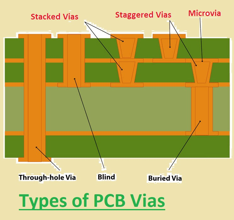
Types of PCB Vias and Their Uses
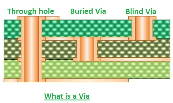
Through-hole Vias
This type of vias is very commonly used. These vias make connections between all layers of the board from top to bottom layer. They are usually used for component mounting and trace connection on layers of the board.
Applications:
● Signal routing: This type of vias routes signals between different board layers.
● Escape routing: it also connects the pinout of surface mount components to the inner layers of the board.
●
Power routing: This via type also routes power and ground currents between different board layers.
Buried Vias
These vais just connect the internal layer of boards. They are confined within the board. Buried vias are used for high-frequency boards since they need accurate signal quality.
Applications:
● High-Density PCBs: Buried vias are used in high-density PCBs to connect inner layers while keeping the surface layers free for component placement.
●
Signal Integrity: They can improve signal integrity by reducing signal path lengths and interference.
Blind Vias
This type of vias connects only the inner layers of a board. They start on the board's upper or lower layer but do not pass through the complete board. These vias are used for high-density boards with limited space.
Applications:
● Connecting surface mount components to inner layers of the board: These vias are used to connect the pinout of surface mount components to the board's inner without going through the top or lower layer.
●
High-density PCB routing: This route signals between different layers of a high-density board without enough space for through-hole vias.
Microvias
They are very small vias and have diameters equal to or less than 0.006 inches. These vias are used for high-density boards with fine-pitch components.
Applications:
● Miniaturization: Microvias are small vias with diameters less than 0.15 mm (150 microns). They are used in densely populated boards and enable the miniaturization of electronic devices.
●
High-Frequency Applications: They are essential in high-frequency and high-speed board designs, like smartphones and high-performance computing devices.
Stacked Microvias
They are two or more microvias configured on each other. These vias connect the internal layers of a board without having to drill through the uppermost or lower layer.
Staggered Microvias
These vias are placed offset from each other. Signal quality is improved, and EMI is reduced by using staggered micro vias.
Thermal Vias
These vias are helpful for heat dissipation from components to the board. These vias are usually more extensive than other vias types and are mostly filled with a thermally conductive material.
Applications:
● Heat Dissipation: They are made to transfer heat away from heat-generating components on a board, like power amplifiers, processors, or LEDs.
Improving Thermal Performance: They are essential for ensuring the effective cooling of components, which is suitable for the reliability and performance of electronic devices.
PCB Vias: What is Via-in-Pad
Via-in-pad (VIP) is a PCB board design method configured directly below the surface-mount component pad. It is helpful for direct electrical connection between the components and the internal layers of the PCB board, which can increase signal quality and thermal operation. This technology is also employed to minimize the board size since it reduces the routing of traces around the component pads.
VIP is also used for high-density boards with fine-pitch components, like ball grid arrays.
Advantages:
● Reduced PCB board size
● Improved signal quality
● Decreases parasitic inductance and capacitance
● Enhanced thermal performance
● Increases routing density
Disadvantages:
● Increased manufacturing complexity
● Potential thermal stress on components
● Expensive
Applications:
● High-density boards with fine-pitch components
● High-frequency board
● Power electronics PCB
● RF and microwave PCB
● Military and aerospace PCBs
● Automotive PCB boards
● Medical PCB
Design Considerations for Via-in-Pad
● The diameter of via must have enough size to handle the required current and minimize overheating.
● The via's location must be the component pad's midpoint to ensure a good electrical connection.
● There must be non-conductive epoxy used in via to avoid shorts and increase the mechanical strength of the pad.
● The component pad must have enough size to accommodate the via without affecting the solder mask coverage.
Via Covering Process for PCB
Why Cover PCB Vias?
● Preventing Contamination: Uncovered vias have a high chance of being contaminated by moisture dust and other environmental parameters, which can cause corrosion, electrical shorts, or decreased performance.
● Improving Solderability: Covered vias provide good solderability, making assembling components onto the board simple during production. The vias are consistently covered with solder due to accurate covering.
● Enhancing Signal Integrity: With the covering of via, designers and engineers can control the dielectric constant of the via, which affects signal quality. That maintains the quality of high-frequency signals flowing in the board.
● Avoiding Solder Bridging: Without via coverage, solder can bridge between neighboring vias or traces during soldering, causing short circuits. With the use of covering we can reduce this problem.
Methods of Via Covering
There are three main methods of via covering:
Via Tenting
It is the simplest and most common technique, where a layer of solder mask covers the via. This saves solder paste from flowing into the via, resulting in a short circuit. It is used for vias that are less than 0.3 mm in diameter.
Via Plugging
This process partially fills the via with a non-conductive material, like epoxy or resin. It is mainly used for vias larger than 0.3 mm in diameter or existing in areas with a high risk of solder bridging.
Via Filling
It involves filling the via with a non-conductive material. It is costly but offers the best protection against solder bridging and other environmental conditions. It is also used for vias in critical components of the board, like power supply circuits and high-speed signal paths.
Here is a comparison of the three methods:
|
Method
|
Advantages
|
Disadvantages
|
|
Via tenting
|
Simple and inexpensive
|
It is not as effective as other methods at preventing solder bridging
|
|
Via plugging
|
Effective at preventing solder bridging than via tenting
|
More expensive than via tenting
|
|
Via filling
|
It is effective at preventing solder bridging and environmental contamination
|
Costly process
|
How Can PCB Vias Impact PCB Design
Printed Circuit Boards are commonly used in electronic devices, orchestrating the intricate dance of electrons that power the modern world. Within board design, one often overlooked but critical component is the via. These small conduits are significant in determining a PCB's functionality, performance, and manufacturability. In this exploration, we discuss the profound effect PCB vias have on the design landscape, revealing how their placement and usage can shape the efficiency and effectiveness of electronic devices. Here are some points that define the effects of the PCB vias on design.
Signal Integrity
PCB vias are essential for signal quality maintenance. Accurately designed and configured vias help to control impedance and signal reflections. Impedance matching is necessary for high-speed digital signals and RF projects. If correctly placed, vias and their effects on signal quality are addressed, which can cause signal degradation, jitter, and decrease data transmission rates.
Board Density
The proper placement of vias can significantly affect the overall board density. During the design of high-density boards or miniaturized devices, vias can be employed to route traces between different layers, saving surface area. The use of blind or buried vias provides even denser layouts, making small size and compact boards.
Thermal Management
Vias can help in thermal management on the board. By accurately placing vias close to heat-generating components, engineers can increase heat dissipation, avoid overheating, and ensure the durability of electronic components.
Layer Count
Vias can affect the number of layers needed for board design. Through-hole vias are very common and link all layers of a multilayer board.
However, blind and buried vias can also decrease the layer count, reduce production expenses, and make board design cost-effective.
Manufacturing Complexity
The via types also affect PCB board manufacturing and assembly. Through-hole vias are easily made and less expensive to make. Blind and buried vias added complexity to the manufacturing techniques due to additional drilling and plating processes.
EMI and EMC Considerations
Vias can affect a board design's electromagnetic interference and compatibility. Incorrectly placed or designed vias can cause undesired antenna effects, resulting in EMI issues. Accurate consideration of via creation and grounding strategies is needed for fulfilling EMI and EMC parameters.
Routing Flexibility
Vias offers routing flexibility by helping designers to make interconnections between different layers. This flexibility is essential in complicated board designs where signal paths should navigate about obstacles or follow specific design parameters.
Important Considerations About PCB Vias
Here are some of the essential considerations about PCB board vias:
Via Type
There are three main types of PCB vias used: through hole vias, buried vias, and blind vias. Through-hole vias link all board layers, but the other two connect just the inner layers. The type of visa used will based on the application and the manufacturing techniques.
Via Size
It is defined by the current carrying capacity and the needed signal quality. Vias must have enough size to carry the required current without causing overheating. Via is also small enough to prevent the circuit's excessive parasitic inductance and capacitance.
Via Placement
During the placement of vias, signal quality issues and thermal issues must be considered. Vias must not be positioned in the path of high-speed signals or close to heat-sensitive components.
Via Density
The density of vias on a board can affect the manufacturability and board cost. Designers must reduce the use of vias whenever possible.
Via Manufacturing
Different board manufacturing techniques have different drilling and plating vias features. Designers must work with their board manufacturer to ensure that the vias in their design can be made successfully.
How to Create a Via in PCB
Here's a step-by-step detail on how to make a via in a board:
Step One: Open PCB Design Software
First of all, start with the opening of your preferred PCB board design software. Altium Designer, OrCAD, Eagle, KiCad, and others are the most used tools. Make a new PCB board project or open an existing one if you add vias to an already-made design.
Step Two: Select the Via Tool
In the PCB design software, there must be a specific tool or option for making vias. Usually, it exists in the toolbar or menu related to routing or board layout. Go for an icon like a via or hole.
Step Three: Place the Via
Press on the via tool to activate it. After that, put the via on the PCB layout by pressing the required location on the board. Board design software mainly helps specify the accurate coordinates where you must place the via.
Step Four: Define Via Properties
After placing the via, there is a need to define its properties. Here are the main properties explained:
● Via Type: Confirm which vias types you need based on your project need
● Via Size: Define the value of the diameter of the via. Based on software settings, that can be defined as either mils or millimeters.
● Via Drill Size: Also define the drill diameter for through-hole vias. Buried and Blind vias can have different drill sizes for different layers.
● Via Layers: It should be confirmed which layers the via connect. In the case of a through-hole, usually, all layers are connected. For other vias like blind and buried, you'll specify the related external and internal layers.
● Annular Ring: Define the annular ring width, the copper pad about the via. It is essential for ensuring accurate soldering and electrical connectivity.
● Clearance: Set the clearance around the via to specify the distance between the via and other board components, like traces and components.
Step Five: Place Vias as Needed
Repeat the process to make more vias for your project design. Based on the software used, you can copy and paste Vias or use the duplicate functions to save time.
Step Six: Route Traces to Vias
You can use PCB design software's routing tools for components to connect and trace with Vias. Route traces from the component leads or other board components to the via. Ensure you follow design guidelines for trace width and spacing to maintain signal quality and manufacturability.
Step Seven: Check Design Rules
Before finalizing the PCB board design, do design rule checks (DRC) to confirm that Vias follows manufacturing and electrical design requirements. The DRC will find any problem, such as unconnected vias, clearance violations, and other potential issues.
Step Eight: Finalize Design
After completing the layout, verifying the connections and solving any design rule faults will save our PCB design project.
Step Nine: Generate Gerber Files
Gerber files board design software is needed for manufacturing the board. Gerber files come with necessary data for the board manufacturing process, like via locations and sizes.
PCB Design Tips for Vias
● Use the correct vias type for the application. As discussed above, each type of vias has advantages and limitations. Like through-hole vias can easily made but cause parasitic inductance and capacitance in the circuit.
Blind and buried vias have a complex manufacturing process but can increase signal quality. Microvias are also challenging but can be employed to make high-density boards.
● Use the accurate via size for the current carrying capacity and the signal signal. The vias' size must be enough to handle the required current without problem. Vias should be small to prevent adding excessive parasitic inductance and capacitance in the board circuit.
● Correct via pad size usage for the drill bit size and the needed annular ring width. Annular rings are around the via. Their width must be 0.25 mm minimum to minimize drill breakout and ensure a good electrical connection.
● Put vias carefully to avoid signal integrity issues and thermal problems. Vias must not be positioned in the path of high-speed signals or close to heat-sensitive components.
● Do not place vias in the middle of large pads. It can cause the pads to lift during the assembly process.
● Vias can connect both sides of a component pad for good electrical performance.
● Plated vais can be used for high-current applications.
● For connection of plane to power or ground, use stitching vias. It helps reduce the noise and EMI.
PCB Design with Vias in Pcbasic
PCBasic is a Shenzhen PCB assembly manufacturer, SMT PCB assembly supplier, PCB board design company, and PCBA provider. It offers online PCB design and manufacturing services and one-stop PCB assembly services. Different design rules for vias are available. Please let us know if you're interested.