Global high-mix volume high-speed PCBA manufacturer
9:00 -18:00, Mon. - Fri. (GMT+8)
9:00 -12:00, Sat. (GMT+8)
(Except Chinese public holidays)
Global high-mix volume high-speed PCBA manufacturer
9:00 -18:00, Mon. - Fri. (GMT+8)
9:00 -12:00, Sat. (GMT+8)
(Except Chinese public holidays)
HomePage > Blog > Knowledge Base > PCB Calculators Explained: What They Do and When to Use Them
A printed circuit board (PCB) layout has to be precisely designed to guarantee dependability, safety, and best performance. Many electrical parameters, including current carrying capacity, resistance, impedance, and clearance, need carefully study to prevent overheating, guarantee signal integrity, and prevent electrical failure.
Fortunately, PCB calculators simplify difficult computations so that engineers may find the proper trace width, impedance, capacitance, and other essential values. This tutorial aims to investigate fundamental PCB calculators, their related formulas, and their suitable uses.
Whether handling high-power circuit design or high-frequency signal traces, such calculators are indispensable in terms of efficiency and lifetime in designing ideal PCB layouts. First, we will evaluate the PCB Trace Width Calculator.
Using a PCB trace width calculator is quite important for the building of a reliable printed circuit board. The calculator computes the trace width to be kept in order to avoid overheating under a given current load. This is a necessary quality to keep.
● Efficient power distribution: Preventing voltage drops and power loss due to resistance.
● Signal integrity: Maintaining the desired electrical characteristics for high-frequency signals.
● Thermal management: Avoid overheating, which can degrade PCB materials and components.
By using a PCB trace width calculator, designers can optimize their circuit layouts for both safety and performance.
The minimum necessary trace width can be computed using an empirical formula offered by the IPC-2221 standard:
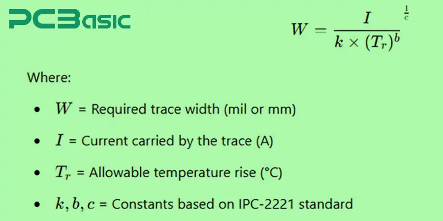
Many factors affect the required trace width.
● More trace to reduce resistance and overheating means a higher current is required.
● Lower allowed temperature rise calls for a larger trace to enable more heat dissipation.
● The thicker copper layers lower resistance, so enabling smaller traces to be used.
● Inner layers must hence carry traces wider for the same current since they dissipate heat more poorly than outer layers.
● Power circuits: Under high current, stop traces from overheating.
● RF and high-speed designs: Appropriate impedance in regard to signal integrity criteria.
● A small PCB design strikes a compromise between carrying capacity and space economy.
A PCB trace width calculator helps designers design dependable and efficient circuits by simplifying difficult calculations.
PCB trace resistance calculator computes the resistance of a trace directly, causing power dissipation and voltage drop. Higher resistance could lead to:
● Rising resistance increases heat loss of energy, lowering efficiency.
● Critical in low-voltage circuits, the voltage drop will affect performance even with small changes in resistance.
● High-frequency signals are more likely to be distorted by undesired resistance.
The designers can also ensure effective power supply delivery and minimize unnecessary losses on their PCB designs by means of trace resistance.
The following formula finds the resistance of a PCB trace:
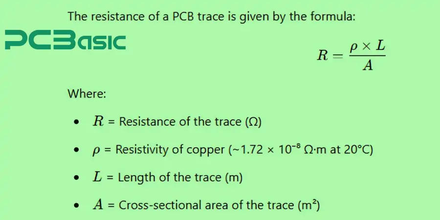
Many elements define the resistance of a PCB trace:
● Longer traces show more resistance.
● Wider and thicker traces have less resistance than thinner ones.
● Standard PCBs contain copper, but the resistance is somewhat changed depending on the copper purity.
● Higher temperatures increase copper's resistivity, generating more resistance.
● Power distribution networks: Reducing voltage drop along high-current paths.
● High-speed signal traces: Reducing resistance-caused signal loss.
● Thermal management: Prevention of excess heat buildup owing to resistive loss.
Employing a PCB trace resistance calculator enables circuit designers to design efficient electronic systems by reducing power dissipation and maintaining steady voltage levels across the entire board.
The PCB trace current calculator finds the maximum current a trace can carry without exceeding thermal limits. Overheating brought on by too strong a current could compromise the integrity of the PCB material and other surrounding parts. Precise PCB trace sizing avoids:
● Dependable electricity without overheating.
● Lowest trace voltage drop.
● PCB's long-term dependability is achieved by avoiding thermal stress.
The IPC-2221 standard computes the maximum current a PCB trace can carry as:
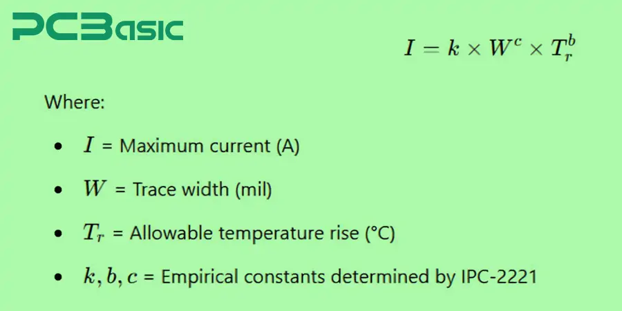
● Track Width, or WWW: Less current will be handled by wider traces before heating them.
● Copper's thickness determines the current flow more so than anything else.
● Increased acceptable temperature rise, TrT_rTr, allows more current but at the cost of PCB material dependability.
● Layer Type of PCB: Inner layers need different trace width computations than outer layers and dissipate less heat.
● Circuit for power supply: Making sure traces can support the given current loads.
● High-power applications: Prevention of overheating in power regulators, motor drivers, and LED circuits.
● Miniature PCB designs: A compromise between board size limitations and trace width.
All such calculations are facilitated by the application of a PCB trace current calculator to enable effective and safe circuit design.
Maintaining signal integrity in high-frequency design depends on the PCB impedance calculator computing the trace impedance. In designs like these, impedance control is especially important since impedance mismatch generates signal reflections, signal degradation, and EMI (electromagnetic interference).
● RF ( Radio Frequency) circuits
● High-speed digital signals ( HDMI, USB, PCIe, etc.).
● PCBs with impedance control for networking and telecommunication
Engineers are guaranteed of the best signal transmissions with minimum loss or distortion by exact measurement of trace impedance.
For a conventional microstrip configuration (a signal trace on a ground plane), the impedance is:
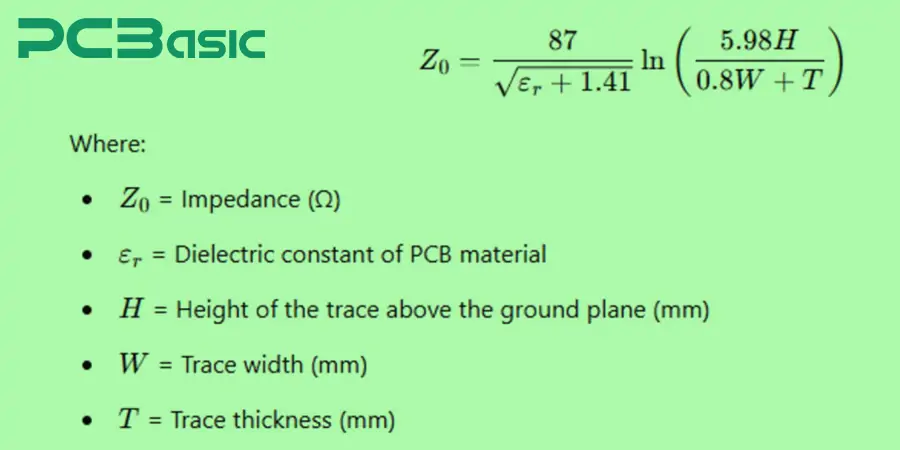
● Dielectric Constant (εr\varepsilon_rεr): Every Material utilized in printed circuit boards (PCBs) possesses some dielectric constant, which affects the velocity at which the signal propagates.
● Trace Width (WWW): An increase in trace width lowers the impedance needed for high-speed signal processing.
● The ground plane height is raised in order to raise the impedance.
● Copper Thickness (TTT): Calculations need to include thin traces since they affect impedance.
● High-speed digital circuits are defined by impedance matching to USB, PCIe, and DDR memory channels.
● In communications systems, maintaining signal integrity: Engineering with radio frequencies and microwaves
● Multiple layer PCBs: Maximizing impedance across multiple PCB layers
PCB impedance calculator enables trace size and material selection optimization, thus providing signal integrity to high-frequency designs.
PCB clearance calculator computes the necessary spacing between conductive tracks, designed to prevent electrical breakdown and arcing. Clearance is especially important for high voltage and high-frequency uses to help satisfy industry standards, dependability, and safety.
● Short circuits caused by incomplete clearance can be arcing-induced.
● Interference of electromagnetic nature (EMI) between neighboring traces.
● Component breakdown caused by unexpected voltage surges.
Following IPC-2221 and ensuring a suitable distance between conductors depending on voltage can be achieved by the designers using a PCB clearance calculator.
The required clearance distance between PCB traces is given by:

● Voltage Level (VVV): More space is required to prevent dielectric breakdown at higher voltage levels.
● Environmental Factors: Impurities, altitude, and humidity can all have an impact on breakdown voltage and call for modifications to clearance.
● PCB Material: Different dielectric material resistances to electrical stress differ.
● Regulations: It is obligatory to comply with safety standards such as IPC-2221, UL 60950, and IEC 60664 for product safety and certification approval.
● High-voltage power circuits: Enough trace spacing prevents arcing.
● Reducing crosstalk and interference between signal traces, RF and high-speed PCBs
● Meeting strict safety requirements for high-voltage applications, automotive and aeronautical electronics
All around, PCB clearance calculators enable designers to maximize life, satisfy industry standards, and design with electrical breakdown protection.
Particularly in high-frequency circuit design, the PCB trace inductance calculator estimates rather important trace inductance. Inductance shapes signal integrity, electromagnetic interference (EMI), and high-speed PCB performance. Trace inductance must be known and controlled if we are to avoid unwanted noise and enable circuits to run as needed.
For a long, straight PCB trace, the inductance is estimated using:
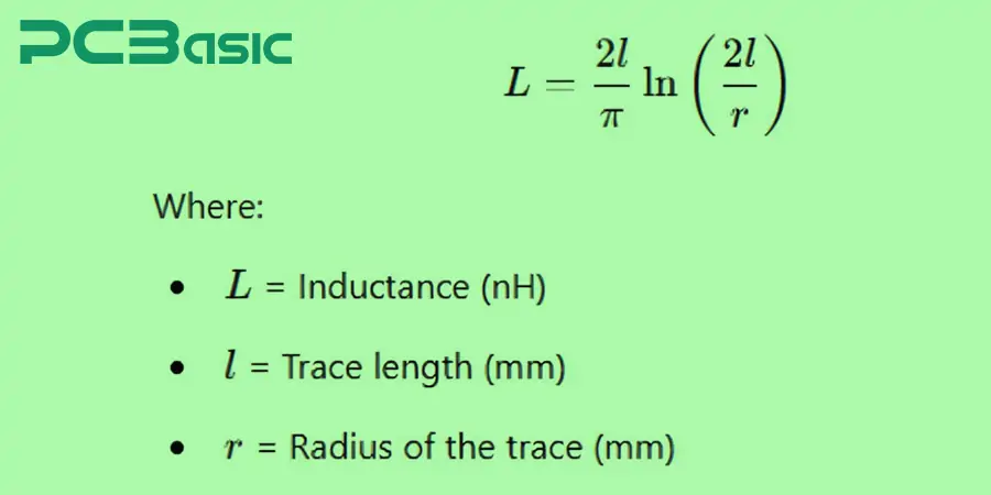
● Trace Length (L): The longer traces are of higher inductance.
● Trace Width (R): Wider traces decrease inductance.
● PCB Layering: Inductance is reduced in multilayer structures with adjacent ground planes.
● Routing and Loop Area: Larger loop areas increase inductance, which leads to greater EMI.
● High-frequency circuits: Control of inductance for preventing undesired oscillation.
● Power delivery networks (PDNs): Reducing inductance to minimize voltage fluctuations.
● RF and microwave applications: For giving accurate impedance matching as well as signal performance.
With a PCB trace inductance calculator, the trace routing may be optimized for maintaining signal integrity and minimizing EMI.
PCB trace capacitance calculator calculates the capacitance between two traces or between a trace and a ground plane. Capacitance affects signal transmission, impedance, and crosstalk and is a critical design consideration in high-frequency, high-speed PCB designs.
The capacitance between a ground plane and a PCB trace is expressed by:

● Dielectric Material (εr\varepsilon_rεr): Higher permittivity materials increase the capacitance.
● Trace Width and Area (AAA): The wider the trace width, the larger the capacitance effect.
● Distance to Ground Plane (D): The shorter the trace to ground distance, the greater the capacitance.
● Signal Frequency: Parasitic capacitance has more effect on higher-frequency signals, impacting performance.
● Reducing signal distortion by means of avoidance of needless capacitance results in high-speed digital circuits.
● Radiofrequency and microwave circuits: Signal transfer via impedance matching.
● Differential pair routing: Matching of capacitance for varied signals.
Circuit performance can be maximized with minimum material and trace spacing by means of a PCB trace capacitance calculator.
Engineers designing good circuits with suitable trace width, impedance, current capability, and spacing would find great use for PCB calculators. Excellent starting point for exact calculations; IPC-2221 standards help to ensure PCB performance and safety.
Although one could do this by hand, online PCB calculators simplify, fast, and error-free such complicated equations. By means of the tools, PCB designers can design efficient, high-performance circuits that not only satisfy industry standards but also application-specific needs, so transcending industry expectations.

Assembly Enquiry
Instant Quote
Phone contact

+86-755-27218592
In addition, we've prepared a Help Center. We recommend checking it before reaching out, as your question and its answer may already be clearly explained there.
Wechat Support

In addition, we've prepared a Help Center. We recommend checking it before reaching out, as your question and its answer may already be clearly explained there.
WhatsApp Support

In addition, we've prepared a Help Center. We recommend checking it before reaching out, as your question and its answer may already be clearly explained there.