Global high-mix volume high-speed PCBA manufacturer
9:00 -18:00, Mon. - Fri. (GMT+8)
9:00 -12:00, Sat. (GMT+8)
(Except Chinese public holidays)
Global high-mix volume high-speed PCBA manufacturer
9:00 -18:00, Mon. - Fri. (GMT+8)
9:00 -12:00, Sat. (GMT+8)
(Except Chinese public holidays)
HomePage > Blog > Knowledge Base > HDI PCBs | High-Density Interconnect PCBs
As the size of electronic devices shrinks and functionality expands, there has never been a greater demand for compact, high-performance circuit boards for the ever-growing needs. Here enters the HDI PCB: a High-Density Interconnect PCB, technology enables designers to pack the more functional power into a smaller space.
Advanced design techniques like micro vias, blind vias, buried vias, and fine trace widths for higher wiring density and superior signal integrity make HDI boards great candidates for applications in such areas as smartphones, tablets, wearables, automotive, and medical electronics.
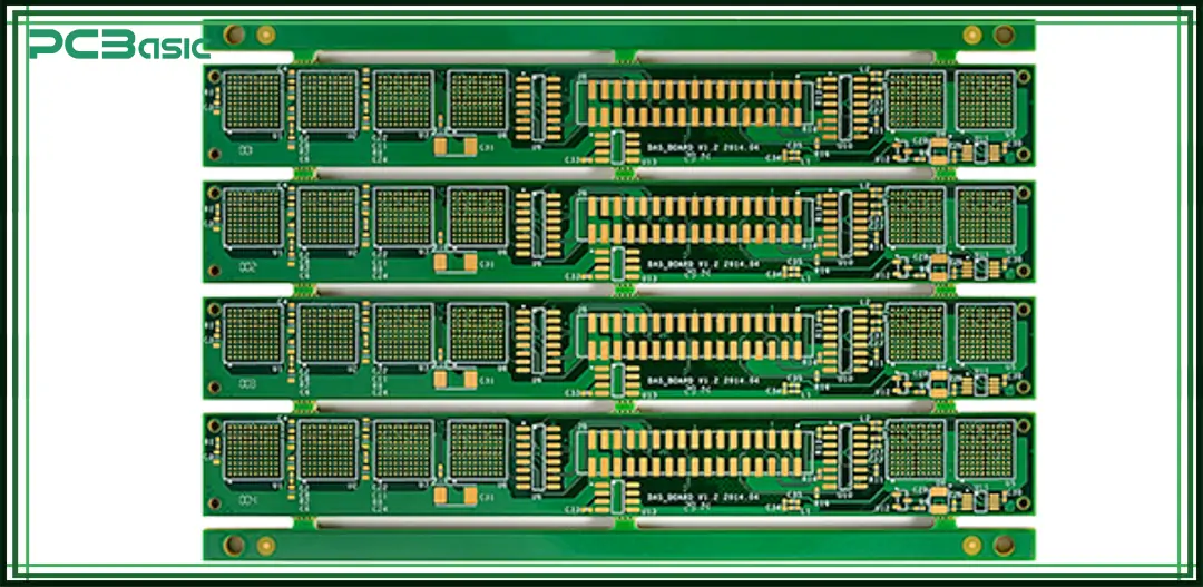
HDI PCB or High-Density Interconnect Printed Circuit Boards are modern circuit boards that offer comparatively more wiring density per unit area than standard PCBs. Designers can build smaller, higher-performance electronics using fine lines and spaces, smaller vias, and higher connection pad density.
With HDI technology, an advanced way of organizing space, it becomes possible to place more active components into a small space. This is accomplished by microvias, blind and buried vias, and multiple layers laminated in sequence. These characteristics make HDIs well-suited for the modern applications of smartphones, tablets, wearables, medical devices, and compact electronics.
As demand for electronic products grew, so did the importance of HDI PCBs in electronics manufacturing. The flexibility in design and advantages of performance have made them the best choice for engineers and HDI PCB manufacturers across the globe.
HDI PCB Stack-up is a specific arrangement of conductive and insulating layers within an HDI board. Unlike the conventional PCB, HDI boards feature combinations of microvias, blind vias, and buried vias to make layer connections, so that routing may have complexity, and component density may increase.
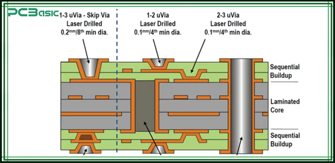
The typical HDI stack-up contains one or more sequences of laminations, thus providing additional routing without increasing the size of the board. Some of the popular configurations include:
• 1+N+1: One microvia layer on each side of a core
• 2+N+2: Two microvia layers on each side providing routing channels
• Any Layer HDI: Microvias can connect to any layer, thus providing maximum design flexibility.
The choice of HDI PCB stack-ups directly relates to the signal integrity, thermal performance, and manufacturability of a device. A well thought stack-up minimizes signal loss while minimizing crosstalk, which supports high-speed data transmission.
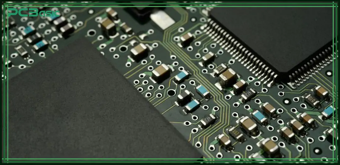
The HDI PCBs have many advantages, thus becoming the favorable choice for modern electronic design. HDI PCB technology, which offers increased density of components and better electrical performance, can be used to build faster, smaller, and much more reliable devices.
Here are some of the key benefits of using HDI boards:
• Miniaturization:
Thanks to the finer traces and microvias, the HDI PCBs support the most compact of layouts and make them ideal for space-constraint applications such as smartphones and wearables.
• Improved Electrical Performance:
Reduced delays and improved signal integrity are the benefits gained from shorter signal paths and reduced parasitic effects and, therefore, higher frequency performance.
• Higher Layer Density:
More layers can be accommodated within HDI stack-ups without increasing the thickness of a board, thus maximizing functionality on a limited surface.
• Flexibility:
Blind and buried vias make HDI PCB designers freer to play with their layouts.
• Improved Management of Heat:
New via structures improve thermal dissipation, making the board more reliable.
• More Reliable:
Laser-drilled microvias are stronger and less prone to failure than microvias mechanically drilled in conventional PCBs.
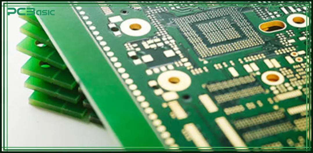
The designing and manufacturing of HDI PCBs is highly complicated processes, unlike standard PCB design and manufacture. Because of their compact sizes and sophisticated configuration, HDI design requires extreme attention to detail, tight tolerances, and control over every step of manufacturing.
Unlike traditional boards, HDI PCB design revolves around high density but without compromising performance. Designers use:
• Microvias and blind/buried vias for reduced layer-to-layer distance.
• Via-in-pad technology saves space and gives users the ability to position fine-pitch BGA components.
• High-speed signal routing techniques that keep signals in that high-density layout intact.
The HDI PCB manufacturing process includes:
• Laser drilling for microvias offers precision that is not achievable with mechanical drills.
• Sequential lamination to build up multilayer stacks one step at a time.
• Advanced inspection and testing to detect minute defects due to the fine features.
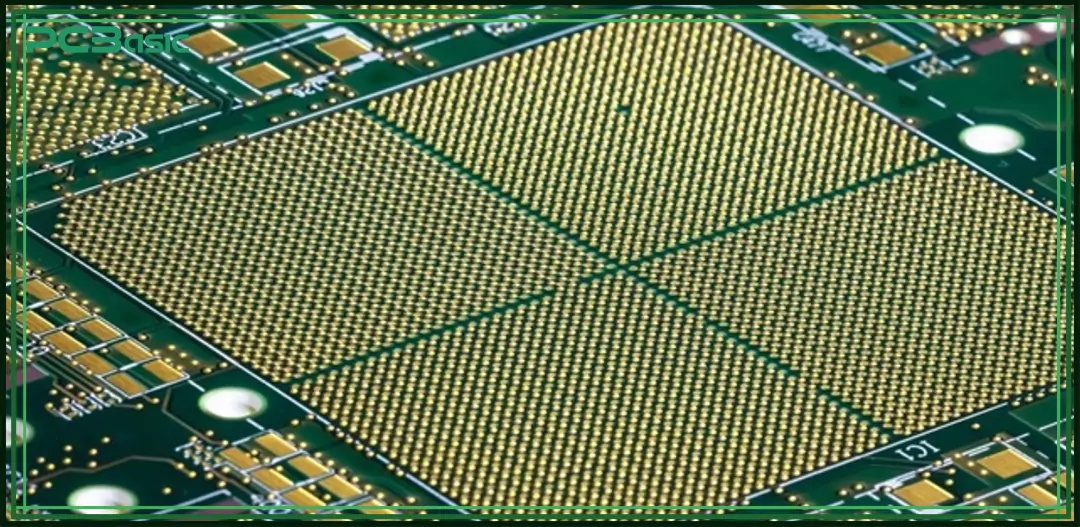
For an HDI board to perform optimally, one must have a good grip on all layout constraints, materials chosen, and manufacturing capabilities. Since an HDI design is aimed for achieving max density and performance in a compact area, proper guideline indeed assures functionality with manufacturability.
Key HDI Design Considerations:
Microvias are a key element of HDI boards. Use them strategically to connect adjacent layers and enable dense component placement without compromising signal paths.
Via-in-pad is one way to make a compact design with good routing efficiency, but it also entails filling and plating the via during manufacturing. This is especially useful for BGAs.
Most HDIs carry high-speed signals; thus, maintaining controlled impedance becomes a must. Pay attention to trace width, spacing, and stack-up configuration to avoid signal degradation.
Involve your HDI PCB manufacturer early in the design phase so that a feasible HDI PCB stack-up can be agreed upon. This will have impacts on impedance, layer count, thermal performance, and costs.
Keep your design within the tolerance limits of your chosen HDI PCB manufacturer. Use standard drill sizes and ensure that your design rules are in sync with those of the fabricator to avoid production delays.
The denser the layout, the more heat is generated. Use thermal vias together with even copper distribution for temperature control and reliability.
The HDI PCB-manufacturing process is heavily complex compared to the standard PCBs due to its finer features and multi-layered nature. Intricate steps of making HDI boards ensure reliability and performance with high-precision equipment and strict process control.
HDI PCBs are made from high-performance base materials like FR4 or advanced laminates with properties supporting fine-line resolution and thermal stability.
Microvias connecting adjacent layers are formed with laser drilling. Unlike traditional mechanical drilling, laser technology is capable of producing the utmost accuracy required in the fine geometries of HDI PCB technology.
In this step, the microvias are copper-plated to establish conduction paths after the drilling has taken place. This is vital since it provides electrical connectivity and long-term reliability.
Layers in an HDI PCB stack-up are built using sequential lamination. This process adds pairs of layers step-by-step, incorporating microvias and buried vias at each stage to support complex interconnects.
Take the high-res image to define patterns for circuits first, and after that, etching to remove the excess copper to get fine geometries of very precise traces. This process enables very high-density routing in HDI PCB Design.
A solder mask is placed to protect the traces, then a surface finish (like ENIG or HASL) is deposited on the pads to ensure good solderability during assembly.
Electrical tests are performed rigorously on each HDI PCB, in addition to inspection with automated optical inspection (AOI) to detect defects in the vias, traces, and connectivity. Thus, all boards are assured to be of quality before delivery.
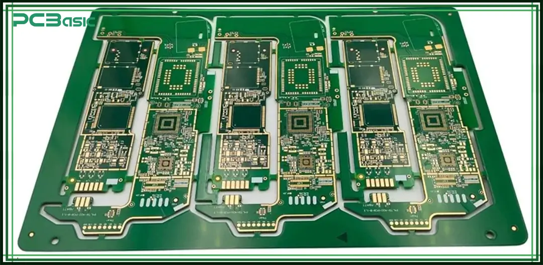
PCBasic is the ultimate solution for top quality HDI PCB assembly, in use by engineers and companies all over the world. With a mix of technical knowledge and responsive service, we manufacture HDI boards that are dependable and high-performance, on budget and on-time.
Specializing in HDI PCB Technology: Expert handling of complex HDI PCB stack-ups and microvia structures.
Fast Prototypes of HDI PCBs: Fast turnaround aligned with your project schedule.
Advanced Manufacturing Equipment: Precision laser drilling, AOI, and control processes are all solid and trusted guarantees for the highest quality.
One-Stop Service: From design support for HDIs to final assembly, it is now under one roof.
Flexible Volume: Whether for single HDI PCB prototypes or volume production, we shall do it.
Reliably On-Time Delivery: Speed comes first, quite not compromising on quality.
Multi-Industry Experience: Automotive, medical, consumer electronics, and industrial.
PCBasic is the reliable HDI PCB manufacturer you can trust for quality, precision, and performance.
HDI PCBs offer more than just being thinner and lighter; they have become an important technology enabling innovations across the sectors. From computer CPUs to smartphones and laptops, HDI technology is used nearly everywhere. Its ability to deliver high performance within a compact footprint makes it essential for modern, space-constrained electronic designs.
All of the steps in HDI PCB fabrication require as much expertise and precision as the design phase, advanced stack-up, and precise manufacturing are a few of the most critical considerations.
PCBasic fits in here. As an established HDI PCB manufacturer, we render complete services from HDI PCB prototyping to full-scale assembly, thus bringing your designs to life with high quality, fast turnaround, and reliability.
Assembly Enquiry
Instant Quote
Phone contact

+86-755-27218592
In addition, we've prepared a Help Center. We recommend checking it before reaching out, as your question and its answer may already be clearly explained there.
Wechat Support

In addition, we've prepared a Help Center. We recommend checking it before reaching out, as your question and its answer may already be clearly explained there.
WhatsApp Support

In addition, we've prepared a Help Center. We recommend checking it before reaching out, as your question and its answer may already be clearly explained there.