Global high-mix volume high-speed PCBA manufacturer
9:00 -18:00, Mon. - Fri. (GMT+8)
9:00 -12:00, Sat. (GMT+8)
(Except Chinese public holidays)
Global high-mix volume high-speed PCBA manufacturer
9:00 -18:00, Mon. - Fri. (GMT+8)
9:00 -12:00, Sat. (GMT+8)
(Except Chinese public holidays)
HomePage > Blog > Knowledge Base > What is a Glass PCB?
As technology improves these days, we are seeing newer innovations around the world. One such advancement you can see nowadays is the use of glass PCBs in the circuit industry. Now you must be wondering, what was the need for developing a new circuit board when the previous one was doing just fine? Well, it is because glass PCBs have numerous benefits compared to ordinary ones. First, traditional PCBs are made with materials like fiberglass and epoxy. On the other hand, glass PCBs use thin sheets of glass material as substrates. Moreover, it has some amazing properties like:
● High thermal stability
● High electrical insulation
● High transparency
All these features combined give us the best result that sets it apart from its counterpart transparent circuit board. However, if you’re still uncertain about its superiority over competitors, then head on to the sections below to learn more about the clear PCB.
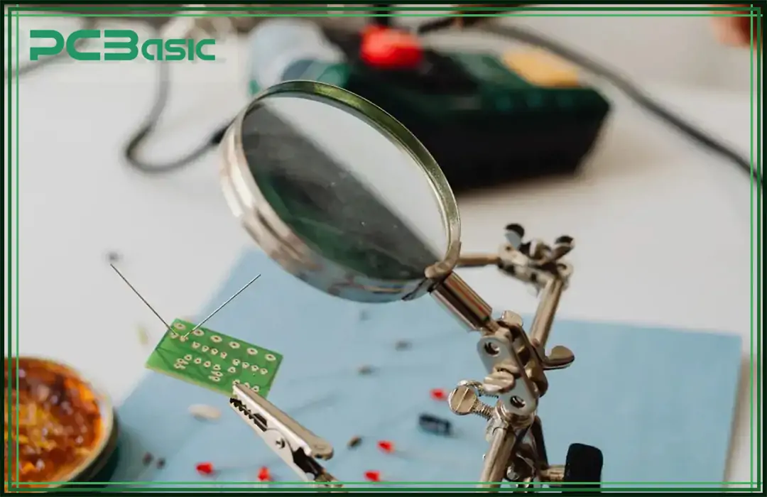
Glass PCBs, also referred to as clear or transparent PCBs, represent a significant innovation in the PCB industry. As said earlier, with making newer devices, we at PCBasic needed something that has more distinctive properties, including superior electrical insulation, high thermal resistance, and dimensional stability. That’s where glass PCBs come into play.
As we studied this further, we saw that it can cater to specific requirements in different industries, including:
● Aerospace
● Telecommunications
● Medical equipment
● Photonics
● Optical devices
● Sensors
Why do glass PCBs have such vast applications? It is because of their precision, reliability, and transparency that makes them optimal for use in niche industries. Not only this, you can see clear circuit boards being extremely compatible with next-generation technology, like high-frequency circuits and miniaturised electronics, where conventional materials might fail.
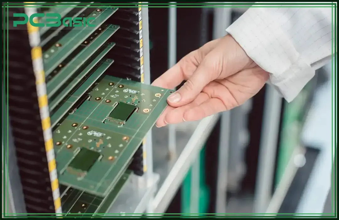
Glass PCBs come in different sizes and kinds, each having its own set of glass substrate nature and a structural feature. Moreover, they are also used for different types of applications depending on how they are prepared and what qualities they hold. So, let’s have a look at different glass PCBs you can see in the market.
The first type of glass PCB uses FR-4, a composite material that combines woven fabric with an epoxy resin binder. Here, for your ease, FR-4 stands for 'Flame Retardant Grade 4,' referring to its flame-resistant properties that protect circuits from heat and electrical shocks. Why is it used? It is because it can withstand temperatures up to 130°C. The picture doesn’t stop here; as we tested, some of its grades can tolerate up to 180°C. If you use this, you can be at peace regarding the moisture control since its water absorption rate is typically below 0.2%.
Glass-ceramic PCBs, as you can get from the name, are a hybrid model between glass PCBs and ceramic. They are recently being used in newer technologies, including:
● 5G telecommunications
● Satellite communications
● Radar systems
They have a low dielectric constant of 2.5 to 4.0, which ensures rapid signal propagation and minimal signal loss, especially critical in high-frequency applications. However, they have a high production cost compared to FR-4 and become brittle, requiring careful handling during fabrication. But, with the advantages it serves in the newer industry, it’s worth its price.
Quartz glass PCBs use high-purity fused silica as the substrate. Fused Silica is known for its ultra-low thermal expansion and excellent optical transparency, making it ideal for specialized high-precision applications. Compared to FR-4, they have the advantage of operating in high temperatures and can withstand temperatures up to 1000°C without losing their properties. Great, isn’t it? But as it can tolerate such high temperatures, it’s expensive to produce them, plus they are also fragile.
These PCBs are built on thin sheets of glass, often less than 0.2 mm thick. This thinness allows them to be used in flexible or ultra-compact devices while still leveraging the inherent benefits of glass. They are ideal for compact designs, including:
● Smartphones
● Tablets
● Flexible OLED displays
● Wearable devices
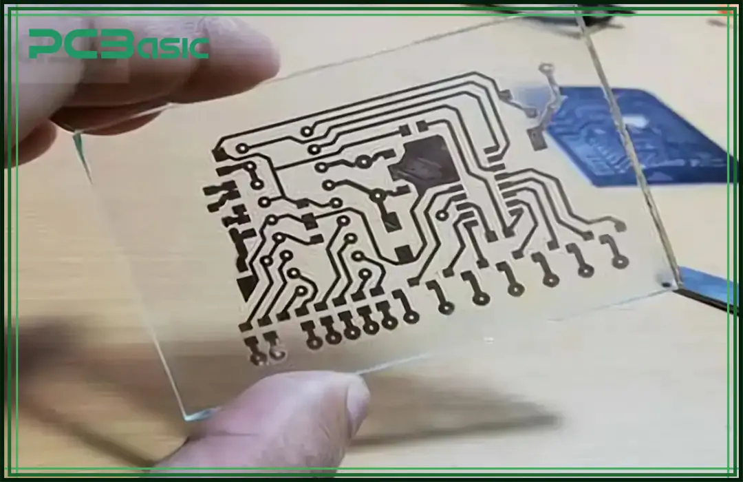
Transparent printed circuit boards (PCBs) are distinct from more traditional PCBs due to their special properties. Their exceptional performance and dependability make them ideal for niche applications. A comprehensive description of glass PCBs is as follows:
Glass outstands others when it comes to resistance to high temperatures and glass substrate. They hold their air even with high-temperature fluctuations. This makes them suitable for applications with fluctuation of or at high and low temperatures.
Glass has a low dielectric constant, so there is little signal loss and interference. It is also an excellent insulator, which makes it ideal for high-frequency and high-voltage applications.
Glass PCBs are transparent, enabling visual examination of components and circuits. This is an inhabitant feature of optoelectronic applications as well as decorative design.
Glass usually does not warp or deform. They provide precision and reliability even in the most exacting of environments.
Glass is unreactive towards many chemicals, making it very suitable for use in hostile environments where chemical attacks may occur. This feature increases the life of glass PCBs in such fields as industry or medicine.
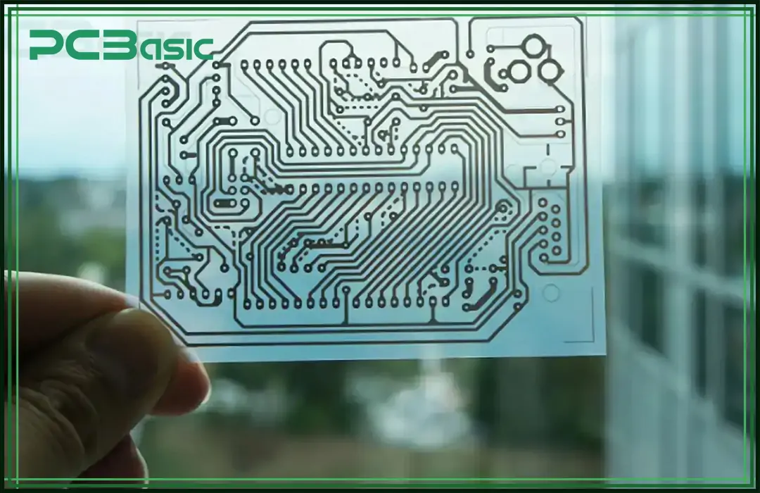
Here are some of the applications of glass PCBs.
Glass PCB is a widely used electronic material for making electromagnetic communication devices (radar communication devices and satellite devices) due to its high dielectric constant. Furthermore, they have extreme temperature and chemical resistance, which makes them trustworthy for use in difficult environments.
Wearable technologies and next-gen diagnostic devices profit from glass PCBs. Being thin and clear, they can be used in new ways to create wearable medical devices, and their ability to manipulate high-frequency signals helps imaging technologies such as MRI and ultrasound systems function more precisely.
Glass PCBs enhance optical properties, improving efficiency, transparency & durability. Thus, they have become an indispensable component of modern photonics applications. Glass PCBs are emerging as indispensable in high-end tech breakthroughs across various industries and applications thanks to their versatility and advanced functionality.
Various electronic applications require glass PCBs for their high thermal resistance, low moisture absorption, and durability. Here is a quick outline of what the process looks like:
The first step is to choose which type of glass PCB you want and select the material accordingly. Depending on the type of PCB, you can choose from:
● Quartz glass (Fused Silica)
● Glass fiber (FR-4)
● Glass-ceramic
● Thing sheet glass
After this, proceed to the selection of your copper foil thickness, which ranges from 18µm to 70µm, depending on the application.
Before applying your conductive layers, make sure your glass substrate undergoes surface preparation to ensure proper adhesion. You can treat them in two ways:
● Ultrasonic Cleaning: Removes any debris, dust, or oils.
● Chemical Cleaning: Uses solvents like acetone or isopropyl alcohol to eliminate surface contaminants.
Then, the circuit pattern is applied to the copper layer through photolithography. Now, you must be confused: what exactly is photolithography? Then let us make it simple for you. It is basically a photoresist application. In this, a layer of photoresist (light-sensitive material) is inserted. There are two categories of that: dry film photoresist and liquid photoresist. Then, the photoresist-coated PCB is exposed to UV light through a photomask that contains the desired circuit pattern.
The glass substrate receives a thin layer of conductive material, typically copper. This can be done using methods like:
● Sputtering or Vapor Deposition (300 nm-thick copper uniform layer is applied by vacuum processing.)
● Electroless Plating: Chemically depositing the copper layer on the PCB eliminates the need for electricity.
A chemical solution removes the hardened photoresist after the etching step, leaving only the final copper circuit on the glass substrate.
If the PCB design locates interconnections between layers of slab stacks, then we usually do precision drilling. For example, laser drilling, because of its precision, is commonly used for glass substrates. A layer of electroless plating then metalizes the vias. We can then cover the resulting clear circuit board with a layer of protective coating, like a solder mask or conformal coating, to shield the circuit from the environment. You can also apply other surface finishes, such as ENIG (Electroless Nickel Immersion Gold), to improve solderability and safeguard the copper.
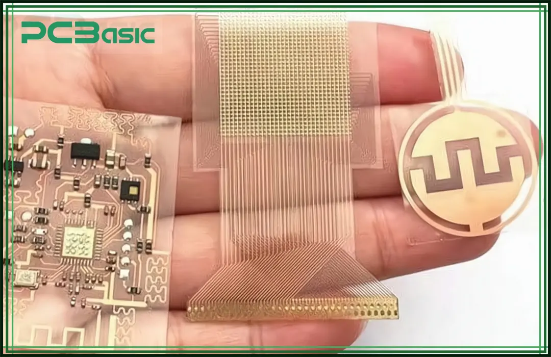
Manufacturing glass PCBs involves several technical and logistical hurdles due to the unique properties of glass and the specialized processes required. Below are the main challenges that manufacturers face when producing glass PCBs:
● Glass PCBs are naturally brittle; they can easily break or shatter when being handled, assembled, or manufactured.
● Drilling, cutting, or laminating poses a higher danger of breaking. Therefore, it is necessary to use specialist equipment, such as drills coated with diamonds or precise cutting machines.
● Glass is harder and more brittle than more conventional materials, making it more difficult to drill holes or machine vias in glass substrates.
● Due to the smooth, non-porous surface of the glass, achieving strong adhesion between the glass substrate and conductive layers can be difficult.
Although people often use the terms "glass PCB" and "clear PCB" interchangeably, they differ in terms of materials, properties, and applications. Here’s a detailed comparison to highlight their differences and similarities:
|
Feature |
Glass PCB |
Clear PCB |
|
Material |
Glass or glass-reinforced |
Transparent polymers |
|
Transparency |
Partial (secondary feature) |
High (primary feature) |
|
Thermal Resistance |
High |
Low |
|
Electrical Properties |
Superior |
Moderate |
|
Durability |
Robust |
Lightweight but less robust |
|
Cost |
High |
Lower |
Glass PCBs represent a significant technological leap in the electronics industry. Their exceptional properties, such as high thermal stability, superior electrical insulation, and transparency, make them indispensable for advanced applications in aerospace, medical devices, and optoelectronics. So, are you also switching to glass PCBs or sticking with the same traditional ones?

Assembly Enquiry
Instant Quote
Phone contact

+86-755-27218592
In addition, we've prepared a Help Center. We recommend checking it before reaching out, as your question and its answer may already be clearly explained there.
Wechat Support

In addition, we've prepared a Help Center. We recommend checking it before reaching out, as your question and its answer may already be clearly explained there.
WhatsApp Support

In addition, we've prepared a Help Center. We recommend checking it before reaching out, as your question and its answer may already be clearly explained there.