Global high-mix volume high-speed PCBA manufacturer
9:00 -18:00, Mon. - Fri. (GMT+8)
9:00 -12:00, Sat. (GMT+8)
(Except Chinese public holidays)
Global high-mix volume high-speed PCBA manufacturer
9:00 -18:00, Mon. - Fri. (GMT+8)
9:00 -12:00, Sat. (GMT+8)
(Except Chinese public holidays)
HomePage > Blog > Knowledge Base > Transistor | Definition, Types, Symbols, and History
Almost all modern electronics are based on a fundamental component known as transistor. The building block of modern embedded systems is also a transistor that acts as a fundamental component to control the processing of data. A transistor is an essential component in Integrated circuits (ICs), microprocessors, and microcontrollers, and in almost every electronic device.
The transistor is a three-terminal semiconductor device that is used to control the flow of current. When voltage or current is applied to the input terminals of a transistor, it controls or amplifies the input signal to generate an output signal. It is made of semiconductor materials such as germanium or silicon. Understanding transistors, their types, transistor symbols, working operation is essential for electrical engineers to design modern electronic systems.
A transistor is an electronic device that controls the flow of current. A Transistor has three terminals known as Base, Emitter and Collector. A typical transistor has two modes of operation, it can act either as a switch or as an amplification device. In switch mode, the transistor allows or permits the flow of current. Whereas, in amplification mode, transistor amplifies the small input signal to generate a larger output signal.
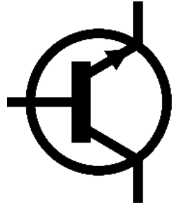
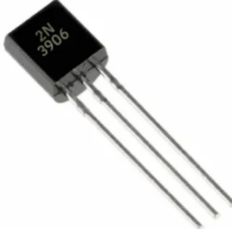
A transistor is made up of three layers of semiconductor material such as silicon and germanium. These layers are either PNP or NPN. The stack of material layers decides the type of transistor, whether PNP transistor or NPN transistor. A typical transistor has three terminals known as the Base, Emitter, and Collector. Such a type of transistor is known as Bipolar Junction Transistor (BJT) transistor. The typical BJT transistor symbol and figure are shown below.
|
|
|
|
|
Transistor layers |
Transistor Symbol |
Transistor package |
Fig-1: Transistor Figure and symbol
Transistors
are classified into three types namely Bipolar Junction Transistors (BJT), Field
Effect Transistors (FET), and Insulated Gate Bipolar Transistors (IGBT). These
transistors are then further divided into subtypes. The details of each type of
transistors are discussed later in article.
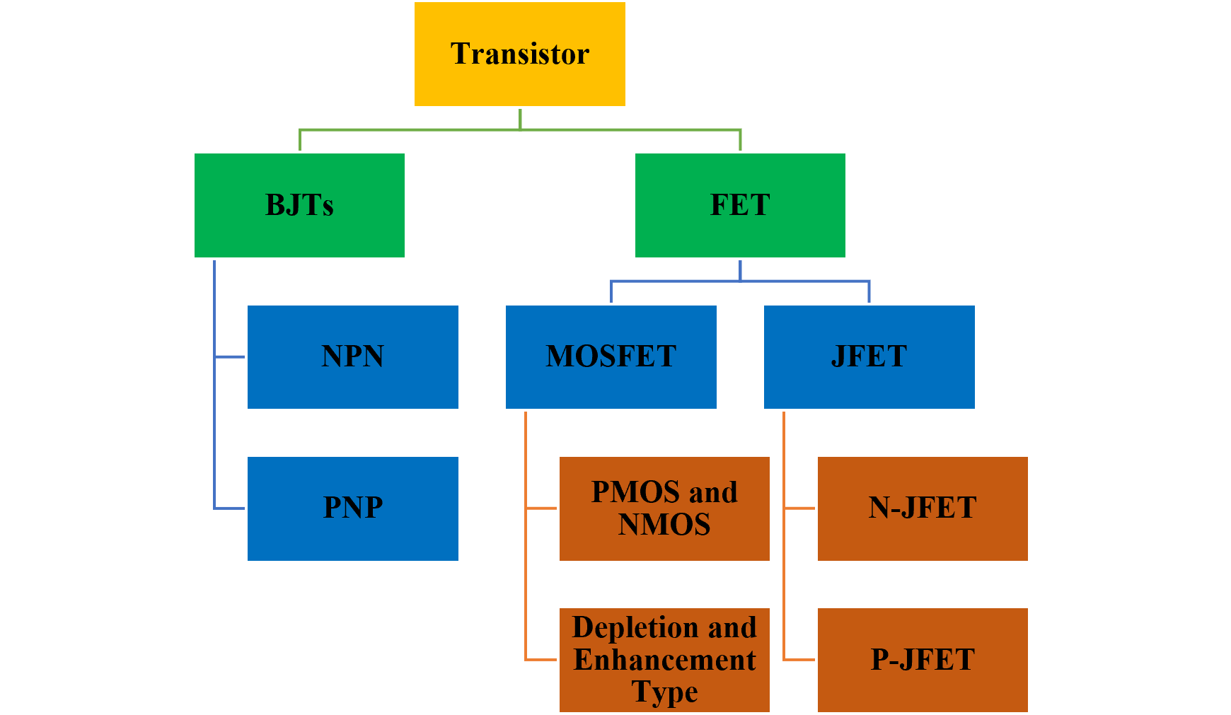
BJT transistor has three terminals known as base, emitter and collector. The flow of current in BJT transistor is due to the free electrons or holes. The small amount of current between the base and emitter terminal of BJT transistor can control the large flow of current between the emitter and collector terminals. BJT transistor is classified into N-P-N and P-N-P Transistors.

Figure 2: BJT Transistors Symbols
In the P-N-P transistor, N-type semiconductor material is sandwiched between two P-type semiconductor materials. This arrangement results in two transistor junctions known as Base-Emitter Junction (Je) and Base-Collector Junction (Jc). In a typical application of transistor, the base-emitter junction is forward-biased and the base-collector junction is reverse-biased. In P-N-P type transistor, current flow is due to the holes as a majority charge carrier.
Whereas, in the N-P-N transistor, P-type semiconductor material is sandwiched between two N-type semiconductor materials. In the N-P-N type transistor, current flow is due to the electrons as a majority charge carrier.
When an input is applied between two terminals of the transistor, it amplifies the input at the output terminals. One terminal of transistor acts as an input and one as an output. The other terminal of transistor acts as a ground. Therefore, three transistor configurations are devised.
1. Common Emitter configuration: In common emitter configuration of a transistor, input is applied at the base terminal of transistor, output is taken at collector and emitter is connected to ground.
2. Common Base Configuration: In common base configuration of transistor, input is applied at emitter terminal of transistor, output is taken at collector, and base is connected with ground.
3. Common Collector Configuration: In common collector configuration of transistor, input is applied at base terminal of transistor, output is taken at emitter, and collector is connected with ground.
FET transistor uses an electric field to control the flow of current. This type of transistor has three terminals gate, drain, and source. FET transistors are unipolar, unlike BJT transistors which are bipolars transistors. FET transistors are extensively used in many applications due to high impedance (up to Mega Ohms), low power consumption, low heat dissipation, and high switching frequency range up to Mega Hertz. FET transistors are classified into two types; MOSFET and JFET transistors.
MOSFET stands for Metal Oxide Semiconductor Field-Effect Transistor. These transistors are widely used in power electronics applications. These transistors are voltage-controlled devices. MOSFET transistor is made of three layers; metal, oxide and semiconductor. The oxide (SiO₂) layer in transistor indicates that it has a thin insulated layer between the metal and semiconductor layers. Therefore, MOSFET uses an electric field to control the flow of current between metal and semiconductor layers. Unlike BJT, MOSFET transistors can only use electronic (N Type) or holes (P Type) as a charge carrier in their operation.

Figure 3: N-Channel and P-Channel MOSFET Symbols
These transistors offer very high input impedance and low output impedance as current is controlled with electric field. The high input impedance of these transistors makes them suitable for power electronic circuits, Integrated Circuits (ICs), Operational amplifiers (Op-Amps), Oscillators, filters, and high switching frequency devices.

Figure
4: Typical MOSFET Through Hole Package
Like BJT, MOSFET Transistors has also three configurations of operation.
1. Common Gate Configuration (Gate is Ground, Input at Source, Output at Drain)
2. Common Drain Configuration (Drain is Ground, Input at Gate, Output at Source)
3. Common Source Configuration (Source is Ground, Input at Gate, Output at Drain)
MOSFET transistors are further classified into Enhancement Type MOSFET, Depletion Type MOSFET, PMOS, and NMOS Transistors.
· Depletion Type MOSFET: Depletion MOSFET transistor also known as D-MOSFET transistor. When current flows between the source and drain terminal of transistor known as a channel. In D-MOSFET the channel is already being constructed in the process of manufacturing. D-MOS transistor normally operates as ON without applying any gate voltage. Therefore, transistor in this condition is referred an ON device. However, when gate voltage is applied at the input of transistor, its channel becomes resistive. Upon increasing the voltage, the channel current keeps on decreasing until the transistor current from the drain to the source stops.
· Enhancement Type MOSFET: Enhancement MOSFET also known as E-MOS transistor. The channel is not already created unlike in D-MOS transistor. In normal condition, no current flows between the drain to source terminal of transistor. However, when the gate voltage is applied to transistor, the current keeps on increasing and makes the transistor channel less resistive.
|
MOSFET Type |
Symbol |
|
N-Channel MOSFET
|
|
|
P-Channel MOSFET
|
|
|
Depletion Type MOSFET
|
|
|
Enhancement Type MOSFET
|
|
·
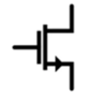
PMOS & NMOS Transistors: Just like MOSFET, PMOS and NMOS transistors also have three terminals gate, drain, and source. The main difference between PMOS and NMOS transistor is that in NMOS transistors, source and drain layers are doped with N-type material. Whereas, in the PMOS transistor, Source and drain layers are doped with P-type material.
|
MOS Type |
Symbol |
|
NMOS |
|
|
PMOS |
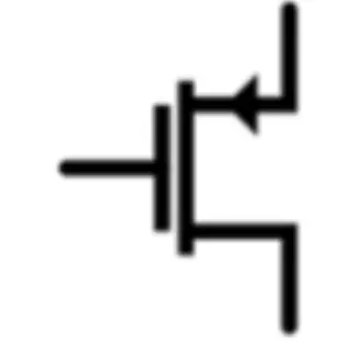
|
JFET is a voltage-controlled device and stands for Junction Field Effect Transistor. JFET is one of the first transistors in FETs and the simplest one. The current flow in JFET transistor is due to the majority charge carriers only, unlike in bipolar junction transistors current flow is due to both majority and minority charge carriers. JFET transistors are classified into N-JFET and P-JFET. It has three terminals gate, source, and drain.
In a normal operation of transistor, when gate voltage is zero, electrons easily travel from source to drain of transistor. However, when the gate voltage is applied across the source and gate terminal of transistor, the P-N junction becomes reverse-biased and increases the width of the depletion layer. This will lead the JFET to pinch off region (Completely OFF).
|
JFET Type |
Symbol |
|
N-JFET |
|
|
P-JFET |
|
A transistor is an electronic device that controls the flow of current. The transistor has two main functions, either used as a switch or an amplification device. Transistor has three modes of operation i.e. cut-off, saturation, and active region. It works as a switch or amplifier based on the operation of region. If a transistor is operated in the cut-off and saturation region, it acts as a switch. However, if it is operated in an active region, it acts as an amplifier.
· Transistor as a switch: With the combination of saturation and cut-off region, a transistor is operated as a switching device. When it is in the cut-off region, the current does not flow at all and a transistor is in reverse biased condition. Therefore, it remains in the OFF state. When it is in a saturation region, current will flow and a transistor is in forward biases condition. Therefore, it will go into the ON state. Transistor has extensive applications where it is operated as switching devices such as blinking of LEDs, DC motors, logic gates, high-frequency drives, precise power regulation, and relays.
· Transistor as an Amplifier: When a transistor is precisely used in an active region, it is operated as an amplifier. The important factor contributing to the amplification is the gain (beta) of the transistor. It is normally mentioned in the datasheet of a transistor. The higher the gain, the higher the amplification of a transistor. Another factor also contributing to the performance of the amplifier is the ratio of input, output voltage, input and output resistance, current gain, and power gain. Transistor as an amplifier is extensively used in radio signals, wireless communication, operational amplifiers, audio devices, instrumental amplifiers, medical devices, and fiber optic communication.
Transistors have revolutionized the modern world. In today’s world transistors are used everywhere from smartphones to rocket engines, modern processors, memory devices, and internet servers.
A typical transistor functions as a switch or amplifier. It is made with three layers of semiconductor materials i.e. N-Type and P-Type. So, how does a transistor work?
A typical transistor has three terminals, base, emitter, and collector. The purpose of the transistor is to control the flow of current. It controls the flow of current by using the principle of charge carriers. The majority of charge carriers are either electrons or holes. The three layers are placed together such that there are two N Types and one P Type is in between them. This makes an N-P-N transistor and vice versa is true for a P-N-P transistor.
The fundamental operation of transistors is based on the base-emitter junction and base-collector junction. These junctions form when a base signal is applied at the base emitter terminal of a transistor. When a small amount of current is applied at the input of transistor, it allows a large current to flow from the base collector junction. This is known as transistor amplification. A transistor in amplification mode is achieved by making the base-emitter junction forward-biased and the base-collector junction reverse-biased.
When no base signal is applied at the input (base-emitter terminals) of transistor, it makes the both base-emitter and base-collector junction reverse-biased. Therefore, no current will flow from the emitter to the collector and the transistor will be in OFF state. A transistor in this region of operation is referred to as a cut-off region.
When a base signal is applied at the input of transistor, it allows the current to flow from the emitter to the collector. Both the base-emitter and base-collector junction in this operation are forward-biased and the collector will be in an ON state. A transistor in this region of operation is referred to as a saturation region.
|
Emitter Junction (Je) |
Collector Junction (Jc) |
Transistor Region of Operation |
|
Forward Biased |
Reversed Biased |
Active Region (Amplification Region) |
|
Forward Biased |
Forward Biased |
Saturation Region (ON State) |
|
Reverse Biased |
Reverse Biased |
Cut-off (OFF State) |
The origin of transistors is rooted back in thermionic vacuum tubes. Thermionic vacuum tubes were invented in 1907 and mainly used for radio technology and radar systems. These were the first type of transistors but consume excessive energy and are bulky in size. These vacuum tubes use an input signal to control the flow of current at the output by using the electrodes.
In October 1925, an Austrian scientist in Canada published a first-ever patent on a field effect transistor. However, his work was ignored at that time due to the lack of research articles published. However, in World War time, bell labs make efforts to produce a pure germanium crystal to use in radar and frequency mixer signals.
In 1947, John Bardeen and William Shockley at Bell Labs, New Jersey, United States invented the first ever working transistor. Later on, in 1958, Bell Labs introduced the MOSFET transistor. The invention of MOSFET has revolutionized modern electronics as it was the first planar transistor in which the drain and source both are on the same surface. The discovery of MOSFET has then widely replaced the conventional transistors in almost all electronics including processors, memory devices, and microcontrollers.
In conclusion, the transistor is one of the major inventions of the 20th century that has changed modern electronics. Modern embedded electronics such as processors, microcontrollers, and digital devices consist of transistors. Transistors are vital components in modern electronics such as radars, fiber optical communication, medical devices, and instrumental amplifiers. Therefore, understanding transistor operation, its working principles, and types is crucial for engineers to design state-of-the-art applications.

Assembly Enquiry
Instant Quote
Phone contact

+86-755-27218592
In addition, we've prepared a Help Center. We recommend checking it before reaching out, as your question and its answer may already be clearly explained there.
Wechat Support

In addition, we've prepared a Help Center. We recommend checking it before reaching out, as your question and its answer may already be clearly explained there.
WhatsApp Support

In addition, we've prepared a Help Center. We recommend checking it before reaching out, as your question and its answer may already be clearly explained there.