Global high-mix volume high-speed PCBA manufacturer
9:00 -18:00, Mon. - Fri. (GMT+8)
9:00 -12:00, Sat. (GMT+8)
(Except Chinese public holidays)
Global high-mix volume high-speed PCBA manufacturer
9:00 -18:00, Mon. - Fri. (GMT+8)
9:00 -12:00, Sat. (GMT+8)
(Except Chinese public holidays)
HomePage > Blog > Knowledge Base > How Surface Mount Technology (SMT) is Transforming Modern Electronics
In the early 1980s, Surface Mount Technology (SMT) began to be applied in the electronics manufacturing industry. It is different from the traditional Through-Hole Technology (THT), which inserts components into the holes on the circuit board, while SMT directly mounts SMD components on the surface of the circuit board. Because the SMT process is more efficient, lighter in weight and lower in cost, this method soon became a new direction for the development of the industry.
Nowadays, electronic products are getting smaller, lighter and have higher and higher performance requirements, which has promoted the wide application of surface mount technology. It can accommodate more components in a limited space, has a faster assembly speed, and can also achieve automation. Therefore, SMT technology is widely used in fields such as consumer electronics, medical equipment, and automobiles.
This article will take you to understand what surface mount technology is, its meaning, advantages, the process of surface mount PCB assembly, common soldering techniques, and the differences between it and traditional through-hole assembly. Meanwhile, it will also introduce how manufacturers like SMT company PCBasic provide reliable surface mount technology process solutions.

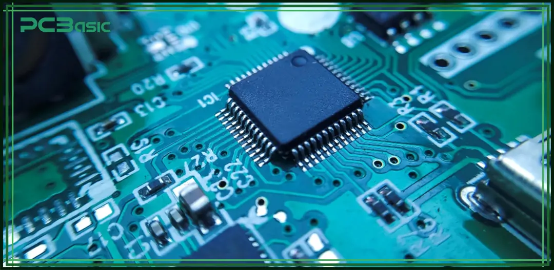
SMT stands for Surface Mount Technology. In SMT, components are directly mounted on the surface of a printed circuit board. The components that are used for directly mounting on the surface of the PCB are known as Surface Mount Devices (SMD). Conversely, in Through Hole Technology (THT), components are inserted into the printed circuit board. This technology is time-consuming and more prone to errors due to human involvement. The SMT, on the other hand, is a completely automated process that reduces cost and time and increases quality and efficiency. However, both surface mount technology and through-hole technology can be used on the same electronic board. This is due to the reason that some electronic components are not suitable for SMT such as high-power components like DC-DC converters and transformers.
The components used in surface mount technology for mounting on the surface of printed circuit boards are known as surface mount devices (SMD). These surface mount devices include several electronic components such as resistors, capacitors, and Integrated Circuits (ICs). All these SMDs come in various sizes and lengths known as packages.
There are different packages of resistors, capacitors, inductors, diodes, and ICs available in the market. Some of the most commonly used SMD packages are:
|
Resistor, Inductor, Capacitor and Diode Packages |
||
|
Package Type |
Size in mm |
Description |
|
0201 |
0.6 x 0.3 |
Tiny size, mostly used in RF circuits |
|
0402 |
1.0 x 0.5 |
Mostly used in sensors and consumer electronics |
|
0603 |
1.5 x 0.8 |
Mostly used in audio devices, defense applications |
|
0805 |
2.0 x 1.3 |
Mostly used in military and industrial applications |
|
1206 |
3.0 x 1.5 |
Often used in power electronic devices |
|
Integrated Circuit (IC) Packages |
|
|
Package Type |
Description |
|
DIP |
Dual In-Line Package is easy to use and is often used in prototype projects. |
|
SOP |
Small Outline Package is compact and is often used in consumer electronics. |
|
TSOP |
Thin Small Outline Package, mostly uses RAM and has a small volume. |
|
QFP |
Quad Flat Package is used to increase board density. |
|
QFN |
Quad Flat No Leads are mostly used in smartphones and industrial electronics. |
|
BGA |
Ball Grid Array is mostly used for microprocessors and controllers. |
|
LQFP |
Low Profile Quad Flat Package is extensively used in the IC manufacturing industry. |
|
TQFP |
Thin Quad Flat Package is often used on small electronic devices. |
|
SOIC |
Small Outline Integrated Circuit, often used in heat dissipation devices such as LDOs and heat sinks. |
|
TSSOP |
Thin Shrink Small Outline Package, used in consumer electronics |
|
PBGA |
Plastic Ball Grid Array, a type of BGA, is mostly used in the development of microprocessors. |
Modern electronic devices, such as mobile phones, laptops, and other electronic gadgets, are getting smarter and lighter with each passing year. This transition has emerged as a new challenge for scientists to make more complex designs in fewer printed circuit board areas. Surface Mount Technology (SMT) has emerged as the best solution to incorporate these challenges due to its ability to fit maximum Surface Mount Devices (SMDs) in less area, resulting in lightweight and smart electronic devices. It is due to this reason that surface mount technology is extensively being used in almost every electronic industry such as medical devices, aviation, defense, and consumer electronics.
Surface Mount Technology uses an automated machine known as a pick and place machine to produce high-volume SMT assembly production, making it ideal for many large-scale SMT companies and electronics manufacturing industries. SMT's extensive automated process enables it to achieve high efficiency and cost-effectiveness. Components used in surface mount technology, known as Surface Mount Devices (SMDs), are very small in size, which not only helps to fit more components in a given printed circuit board (PCB) but is also beneficial for high-frequency circuits. Due to these reasons, large-scale electronic manufacturing industries mostly use SMT technology to manufacture compact, lightweight, smart, and high-quality electronic devices through efficient surface mount PCB assembly.
Surface Mount Technology offers numerous advantages over through-hole technology, resulting in a major shift in the printed circuit board manufacturing industry to choose surface mount technology. Some of the advantages are;
• In SMT, components are directly mounted on the surface of the electronic board, unlike in THT, where components are drilled into the printed circuit board. This feature of SMT enables the assembly of components on both sides of a printed circuit board, making the more complex designs fit in a smaller area.
• Unlike through-hole components, surface mount devices are very small in size, resulting in a maximum number of components to fit on an electronic board.
• The assembly process of surface mount devices is expeditious with the use of a fully automated pick-and-place machine, resulting in high-volume production. The automated assembly process of SMT also enables fast production, high efficiency, and the least margin of error.
• Signal integrity is one of the critical challenges in today’s modern electronic designs. In SMT, the components are smaller and mounted on the surface of the electronic board, resulting in less distance for signals to travel. This improves the problems of crosstalk between signals and reduces inductance and capacitance. Therefore, surface mount devices are ideal for high-frequency circuits.
• The automated pick-and-place machines enable high-volume production, resulting in reduced overall manufacturing costs.
 About PCBasic
Time is money in your projects – and PCBasic gets it. PCBasic is a PCB assembly company that delivers fast, flawless results every time. Our comprehensive PCB assembly services include expert engineering support at every step, ensuring top quality in every board. As a leading PCB assembly manufacturer, we provide a one-stop solution that streamlines your supply chain. Partner with our advanced PCB prototype factory for quick turnarounds and superior results you can trust.
The process that mounts the surface mount devices onto the surface of the printed circuit board is known as the SMT assembly process. There are four main steps in the SMT assembly process. Each step is explained as follows.

Solder paste is a type of mixture that is made up of solder powder and flux. This mixture is used to connect surface mount devices like resistors, transistors, inductors, and ICs to the electronic board assembly. In the first step, solder paste is applied to the pads available on the PCB. This is done by a thin sheet with pre-cut holes known as a stencil.

In the 2nd step, surface mount devices such as resistors, capacitors, and ICs are picked and placed onto the pads of the PCB using an automatic pick-and-place machine.

At this point, components are exactly placed onto the surface of the PCB using a pick-and-place machine. In 3rd step, the Printed Circuit Board is now passed through a heating oven known as a reflow oven. This makes the solder paste melt and solder to form an electrical connection between different components. In the reflow oven, the temperature is maintained such that the solder paste is accurately soldered to the components. The temperature is programmed as per the reflow profile.

In
this step, visual inspection is carried out using the X-ray machine to identify
any soldering faults and any other defects.

In the final step, PCBs undergo a rigorous cleaning process to eliminate any flux residues left after the reflow soldering process.
In the printed circuit board manufacturing industry, mostly two techniques are employed known as wave soldering and reflow soldering.
1. Wave Soldering
Wave soldering is not as common as reflow soldering. This technique is mainly used for Through Hole Technology but it can be used for SMT.
Step 1: Mount the components on the PCB
Step 2: Pass the PCB over a wave of molten solder
Step 3: Solder wires and form an electrical connection
Step 4: Use air/water to cool the PCB.
This technique is less efficient and more prone to errors as compared to reflow soldering.
2. Reflow Soldering
Reflow soldering is one of the most widely used techniques in surface mount technology. It is used for high-volume production and has the least margin of error. This technique is mostly used for surface mount technology. The reflow soldering process has the following steps.
Step 1: Apply the solder paste using stencil printing
Step 2: Pass the PCB to the pick and place machine for the placement of components
Step 3: The printed Circuit Board is now passed through a heating oven known as a reflow oven. This makes the solder paste melt and solder to form an electrical connection between different components. The reflow process typically has four stages
a) Preheat
b) Soak
c) Reflow
d) Cooling.

Surface Mount Technology (SMT) and Through Hole Technology (THT) have become the industry standards in printed circuit board manufacturing. Both these technologies are primarily used for assembling electronic components on the printed circuit board. However, these technologies have distinct features, uses, processes, advantages, and applications.
Table I: Surface Mount Technology VS Through Hole Technology
|
Aspect |
Surface Mount Technology (SMT) |
Through Hole Technology (THT) |
|
Technique |
SMT directly mounts the components on the surface of the PCB |
THT inserts the components on the PCB via drilled holes. |
|
Assembly Process |
SMT is a fully automated process using a machine known as a pick-and-place machine. |
THT is mostly done manually or by an automated machine |
|
Component Placement |
SMT allows for placing the components on both sides of the PCB |
THT only allows components to be inserted on a single side |
|
Board Volume |
More components can be fit in a given area. |
A smaller number of components can be assembled in a given area as compared to SMT. |
|
Mechanical Stress |
SMT offers fewer mechanical bonds as compared to THT because THT components are inserted through holes. |
THT offers a strong mechanical bond between components and the PCB |
|
Components suitability |
SMT is suitable for SMD devices such as resistors, capacitors, ICs, BGA, microcontrollers, and microprocessor ICs |
THT is only suitable for high-power components such as DC-DC converters and transformers. These components are bulky and are not suitable for SMT. |
|
Cost |
SMT's initial cost is higher due to the procurement of automated machines like pick and place machines. However, overall manufacturing cost is less as compared to THT. |
THT initial cost is lower due to the manual process. However, overall manufacturing cost is higher than SMT. |
|
Repair and Reworks |
In SMT, it is difficult to repair and rework once manufactured. |
In contrast, it is relatively easy to do repairs and reworks Through through-hole technology (THT) |
When pursuing reliable, efficient, and high-quality SMT assembly services, PCBasic is a trusted partner in the electronics manufacturing industry. With over 15 years of experience in PCB design and project management, PCBasic can provide end-to-end support for both small-batch and large-batch surface mount technology production.
• Expertise You Can Trust:
Backed by seasoned engineers and in collaboration with PhD teams from top universities, PCBasic drives continuous innovation through industry-academia research.
• Dual Factory System:
Our Shenzhen facility specializes in quick-turn small-batch runs, while the Huizhou factory handles high-volume production with streamlined processes.
• Vertical Integration:
We operate our own stencil and fixture factory, offer CNC precision parts processing, and deliver stencils within 1 hour, ensuring fast response and complete process control.
• Smart Component Management:
With an intelligent electronic components central warehouse, PCBasic ensures a stable supply of original and genuine parts.
• One-Click BOM & Instant Quoting:
Upload your BOM file and receive fast, accurate pricing through our automated system—perfect for rapid prototyping and volume manufacturing.
• Certified for Excellence:
As a national high-tech enterprise, PCBasic is fully certified with ISO13485, IATF 16949, ISO9001, ISO14001, UL, and is a proud IPC member. We hold over 20 patents for quality inspection and production systems.
Whether you're developing medical, automotive, consumer, or industrial electronics, PCBasic delivers surface mount PCB assembly solutions with precision, speed, and quality you can count on.
To sum up, surface mount technology is the game changer in the printed board circuit manufacturing industry. Surface Mount Technology has emerged as the best solution to incorporate maximum surface mount devices (SMDs) in less area, resulting in lightweight and smart electronic devices. SMT enables the industries to produce high volume production, making it less costly and increasing efficiency.

Assembly Enquiry
Instant Quote
Phone contact

+86-755-27218592
In addition, we've prepared a Help Center. We recommend checking it before reaching out, as your question and its answer may already be clearly explained there.
Wechat Support

In addition, we've prepared a Help Center. We recommend checking it before reaching out, as your question and its answer may already be clearly explained there.
WhatsApp Support

In addition, we've prepared a Help Center. We recommend checking it before reaching out, as your question and its answer may already be clearly explained there.