Global high-mix volume high-speed PCBA manufacturer
9:00 -18:00, Mon. - Fri. (GMT+8)
9:00 -12:00, Sat. (GMT+8)
(Except Chinese public holidays)
Global high-mix volume high-speed PCBA manufacturer
9:00 -18:00, Mon. - Fri. (GMT+8)
9:00 -12:00, Sat. (GMT+8)
(Except Chinese public holidays)
HomePage > Blog > Knowledge Base > What are Castellated Holes on a PCB?
PCB manufacturing has experienced massive technological advancement. Modern designers have made various advancements in mounting new PCBs to meet their clients' needs. Previously plated through holes and vias have been used to create interconnections between several layers of the PCBs. However, this has not been enough to help interconnect PCBs to PCBs.
During the design process, you find that certain functionality can be achieved by borrowing an existing PCB and integrating it into your design to complete your idea. For example, if you are making an IoT project that involves WI-FI connectivity, you do not need to design the WIFI circuit from scratch. Borrowing readily available modules like the ESP32-WROOM-32E is enough. But one will wonder how the WI-FI module is connected to your design. This is where castellated PCBs come in to solve the situation. Therefore, the ESP32-WROOM-32E is an example of a PCB module that embraces the castellation technology. This article will introduce castellated PCBs and help you understand them in detail.

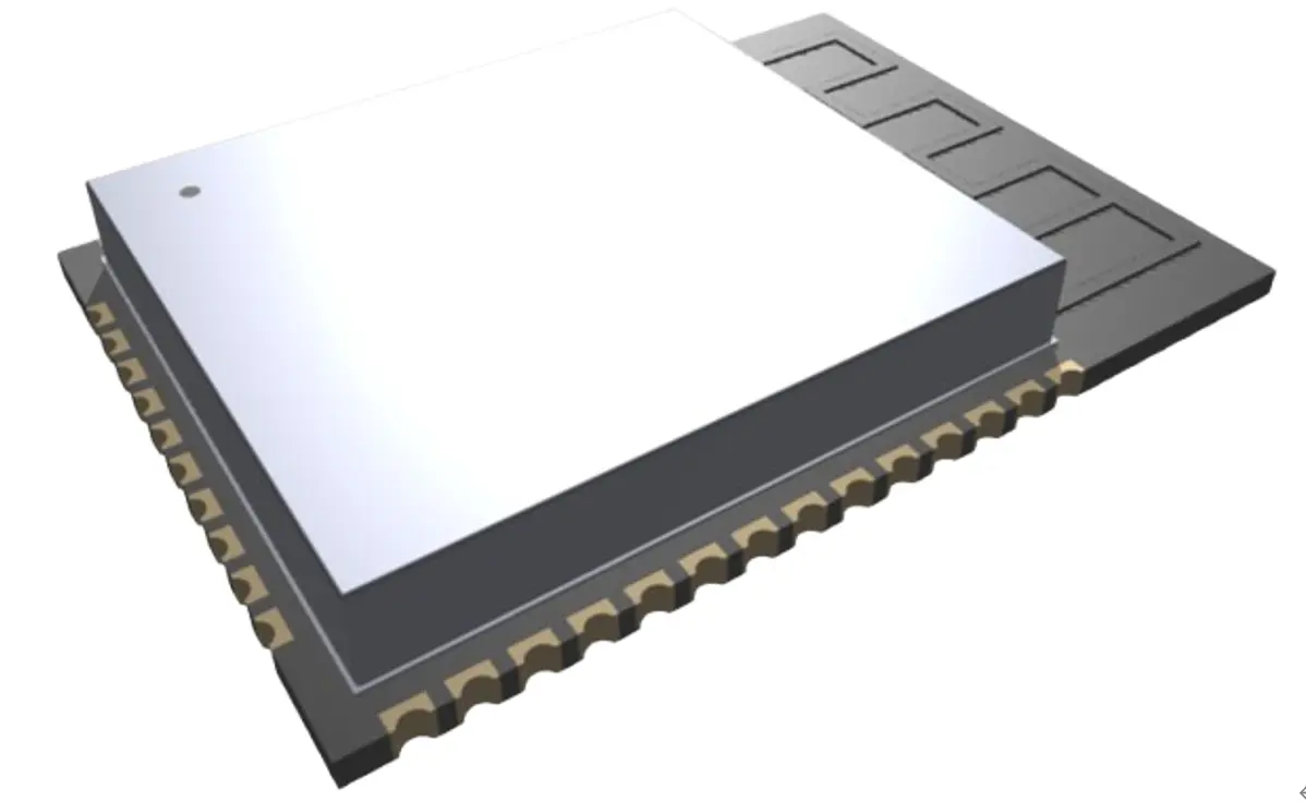
Figure 1: ESP32-WROOM-32E Module with Castellated Holes
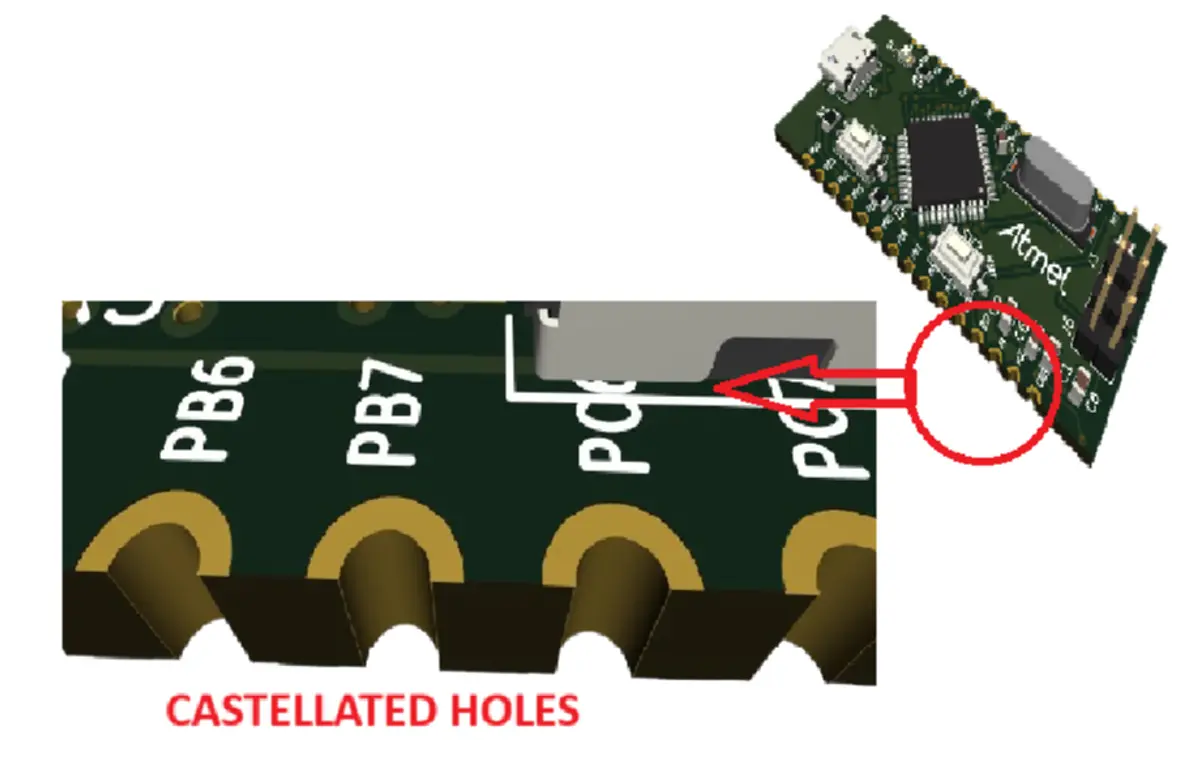
Castellated PCBs are PCBs designed with unique mounting holes known as castellated holes. The castellated holes are placed on the edge of the PCBs. These holes allow designers to mount PCBs on top of another PCB through a process known as board-to-board soldering. Like the through holes and vias, the castellated holes are plated to improve conductivity. Castellated holes are generally halved through holes. The features are preferred when surface mount technology is used.

Figure 2: Castellated Holes on a PCB Periphery
With castellated holes, PCBs gain various benefits that would make them suitable for multiple uses, such as:
· Integrating modules to host PCBs: Various modules such as GPRS, GPS, Wi-Fi, and Bluetooth come with castellation holes, which make it possible
· Prototyping processes: With castellated holes, designers and innovators are guaranteed simplified product testing, prototyping, and assembly.
· PCB miniaturization possibility: With the advent of castellated PCBs, it has been possible to develop modules that can be fitted in limited areas, thus reducing PCB sizes.
· Improved PCB durability: Castellated holes have improved the mechanical structure of PCBs, thus making them more durable.
· Improved electrical stability: PCBs with castellated holes have better electrical properties. The plated castellated holes have improved the interconnect between PCBs, thus improving electrical stability.
Castellations in castellation PCBs can be classified into full, partial, and staggered castellations.
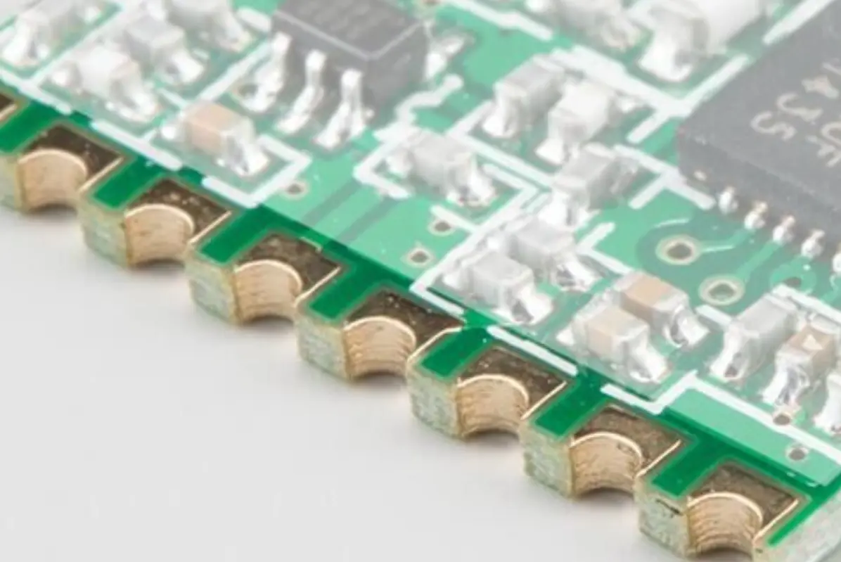
Full castellations in PCBs are formed by halving the plated through holes placed on the PCB's edge. This forms fully plated semi-circular holes (see Figure 2). The complete plating is intended to improve mechanical robustness and electrical continuity.
To form full castellations, complete holes are made near the edge of the PCB. The edge is milled, leaving half of the through-hole intact. Finally, the entire formed shape is plated using copper.
Full castellations are used in the following areas:
· PCB Edge soldering: Sometimes, as a designer or a manufacturer, you want to attach some modules, such as SIM800L cellular module, ESP32 WI-FI modules, etc., to your host PCB, and full castellation comes to your rescue.
· Grounding: Full castellations are used as shields in areas where electromagnetic and radio frequency interferences are given priority.
· Electrical interconnects: Full castellation is suitable for manufacturing stackable boards by ensuring electrical continuity.
· Prototyping and testing: During the project's early design, prototypes employ full castellations techniques that provide test points for testing the performance of the PCBs or even connecting external PCBs that could help during testing.
Partial castellations are borrowing from full castellations. The difference is that, for partial castellation, the u-shaped engravements are not fully plated. This type of castellation has shallow depth, too. Unlike the full castellation, it does not cut through the entire PCB thickness.
Partial castellations are used in PCBs that have the following:
· Space constraint: Some PCBs have limited space, prohibiting full castellations; at this point, partial castellation is necessary.
· Less critical interconnects: Partial castellations are used where a robust mechanical connection is not vital. They are preferred because they reduce the cost of the PCB.
· Flexible circuit signal points: Partial castellations are used in flexible circuits since they provide anchor points for weaker signals.
Staggered castellations have been plated halved through holes placed irregularly along the PCB edge. Unlike whole and partial castellations, where the engravements have uniform depth, height, and positioning, staggered castellations have different variations of similar features. The castellations can be fully or partially plated.
Staggered castellations are used in the following areas:
· HDI: HDI (High-Density Interconnect) PCBs have many components in a limited area. These multilayer PCBs have a limited interconnect area. Staggered castellations are utilized to ensure interconnection.
· Breakout boards: Staggered castellations are adapted in modular PCBs where connectivity might be needed at any given time without interfering with the strength of the same board.

In addition to the three types of castellation in PCBs, designers use three configurations in castellated PCBs: single-row, double-row, and interleaved castellations.
The most common configuration of castellations is a single-row castellation, which consists of a single row of notches located along the edge of the PCB. Every castellation is independent and has copper plating to enhance connectivity with other PCBs.
Single-row castellations are easy to design and offer robust mechanical connections, adequate electrical properties, an easy soldering surface, and excellent connector compatibility. However, they have limitations, such as limited contact surfaces, as a single row offers limited castellations for connectivity and is unsuitable for HDI and other complex PCBs.
Double-row castellation has two parallel layers of notches at the edge of the PCB. The number of contact points is doubled, increasing connectivity while maintaining the PCB size.
It generates a compact design suitable for HDI, interfacing daughterboards to motherboards and more complex devices involving numerous communication protocols. However, this type of configuration has limitations due to high manufacturing costs, complex design, and assembly difficulty.
In an interleaved castellation configuration, the castellations are staggered at the edge of the PCB in either two or more rows. In other words, the arrangement assumes a zigzag pattern. This increases the connectivity surfaces while maximizing the spacing.
Interleaved castellation offers an increased connection surface, routing flexibility, and better signal integrity than others. However, it is relatively expensive and complex during assembly, and more advanced manufacturing techniques are required.
Castellated PCBs require advanced knowledge, techniques, and equipment to manufacture. Before manufacturing, you need to consider the following during the design of your project:
· Specifications: the castellated hole's lowest diameter should be 0.6mm, and the highest diameter should be 1.2mm. The application area determines the size of the selection. The whole must be plated with copper to enhance conductivity and solderability.
· Short circuit prevention: The surrounding castellated holes are covered with a solder mask to prevent short circuits. Solder masks also improve the board's appearance.
· PCB edge plating: The PCB edge must be copper-plated to ensure that the PCB has a conductive surface.
· Make mouse bites: Castellated PCBs have mouse bites at the edges. These tiny perforations enable easy attachment and detachment of the PCBs without interfering with signal integrity.
The following areas are where castellated PCBs find use:
· Testing and prototyping: During manufacturing, castellated PCBs are used to test the boards to ensure they meet the expected requirements.
· Used in IoT Devices: Devices such as the GPRS. GSM, GPS, Bluetooth, and Wi-Fi modules adopt castellated technology for easy integration.
· Power management systems: BMS systems that require seamless connection adopt castellated PCB technology.
Besides the many advantages and usage, Castellated PCBs come with various challenges. The manufacturing process is very complex. When not handled with enough care, castellation plating can be damaged. This technology is not an option for high-current PCBs, which means castellation PCBs have design limitations. Another challenge is the soldering issue. If not keenly soldered, the castellated holes can be blocked.
Castellated PCBs have found a place in the world of modern electronics. Their advent has made it possible to interconnect PBs. With their versatility, IoT, embedded systems, prototyping, and innovation have met the expected quality. However, designers need to have prior knowledge to help them get the most out of the castellated PCB technology.
Hobbyists and designers have benefited from castellated PCBs' electrical and mechanical robustness. Their easy solderability, thermal conductivity, and mechanical strength have enabled better and more advanced projects. Please explore our website, PCBASICS, to learn about the services we offer regarding castellated PCBs.

Assembly Enquiry
Instant Quote
Phone contact

+86-755-27218592
In addition, we've prepared a Help Center. We recommend checking it before reaching out, as your question and its answer may already be clearly explained there.
Wechat Support

In addition, we've prepared a Help Center. We recommend checking it before reaching out, as your question and its answer may already be clearly explained there.
WhatsApp Support

In addition, we've prepared a Help Center. We recommend checking it before reaching out, as your question and its answer may already be clearly explained there.