Global high-mix volume high-speed PCBA manufacturer
9:00 -18:00, Mon. - Fri. (GMT+8)
9:00 -12:00, Sat. (GMT+8)
(Except Chinese public holidays)
Global high-mix volume high-speed PCBA manufacturer
9:00 -18:00, Mon. - Fri. (GMT+8)
9:00 -12:00, Sat. (GMT+8)
(Except Chinese public holidays)
HomePage > Blog > Knowledge Base > PCB Warpage: Causes, Effects, and Prevention
Warped PCBs can quietly wreck your entire assembly line. One minute, everything looks fine. The next moment, you are chasing down open solder joints, lifted pads, and rejected boards.
PCB warpage isn’t some harmless curve. It wrecks yield, messes with precision, and chips away at long-term reliability.
So, what’s behind it? Sometimes, the material. Other times, the process. Usually, both. But the real issue isn’t spotting a warped board—it’s knowing how to measure it the right way. And better yet, how to stop it from happening again.
That’s what this article is all about. From the basic definition to the physics behind the bend. From the root causes in design and manufacturing to real-world impacts during reflow. You’ll also learn how to detect it, measure it accurately, and fix the problem before it ruins a production run.
Let’s break it down—without the fluff.
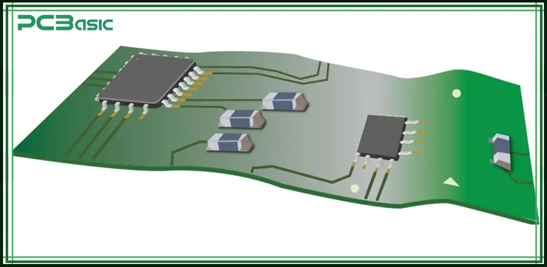
PCB warpage is the physical distortion of a circuit board. Instead of lying flat, the board bends, twists, or bows. This can happen during manufacturing, storage, or reflow. And it doesn’t take much—just a small amount of warpage can throw off your whole SMT process.
Technically, it’s a deviation from the board’s original flat shape. IPC standards define acceptable warpage limits. For surface mount, it’s usually 0.75%. For through-hole, 1.5%. Beyond that, problems start stacking up fast. However, limits vary by thickness and application. In simpler words, bent PCB means a broken process.
No one single thing causes a board to warp. It’s often a mix. Materials, design, and handling—all play a role.
Let’s look at the biggest culprits:
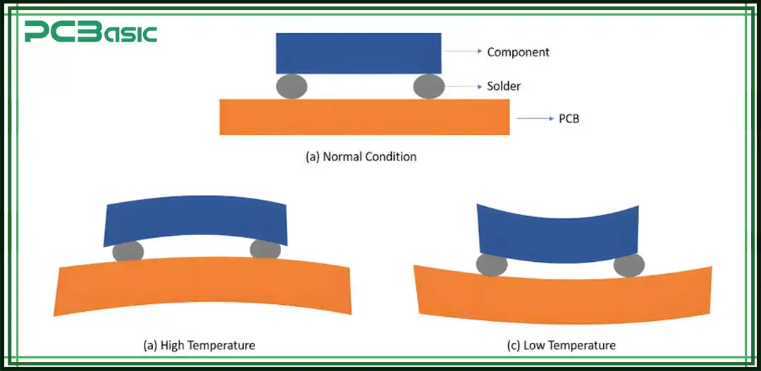
A PCB is made of layers. FR4, copper, prepreg, solder mask. If those layers don’t expand and contract evenly with heat, stress builds up. That stress bends the board. Boards with unbalanced stacks are more likely to twist or bow.
Copper heats up differently than fiberglass. If you have got a dense copper area on one side and almost nothing on the other, the board expands unevenly. That pulls the board out of shape—especially during lamination or reflow.
During lamination, high heat and pressure are applied. If the pressure isn’t even—or the temperature’s off—internal stress gets trapped. You might not see the warpage right away. But once the board hits reflow, it shows up.
FR4 is hygroscopic. It soaks up moisture like a sponge. If the board isn’t baked or stored properly, that moisture expands rapidly under heat. The sudden expansion causes internal delamination or micro-cracks that push the board into a curve or twist.
Big or dense parts placed unevenly on one side of the board can cause stress during soldering. The weight, combined with heat, bends the board down. This is especially common in reflow ovens with uneven thermal profiles.
Are you stacking boards flat without spacers? Or storing them vertically? And exposing them to heat or pressure? All of these lead to bent PCB. Handling matters, too. Dropping a board, flexing it while picking it up, or leaning tools on top. It all adds up.
A warped PCB doesn’t sit flat. That alone is a problem. But it gets worse during assembly.
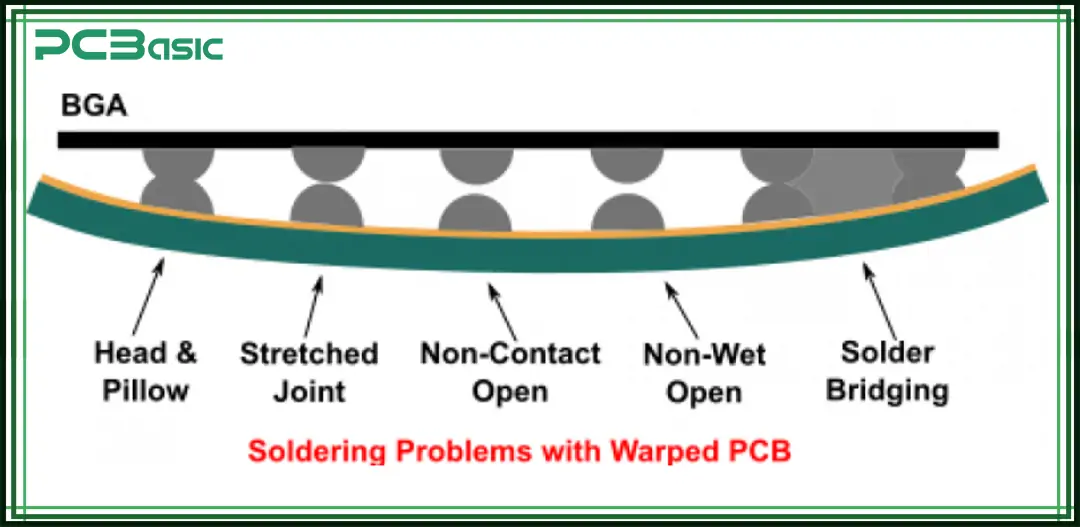
SMT needs precise alignment. Warped boards lift pads off the solder paste. That creates weak joints—or no joints at all.
Bridges, open and cold joints—they all trace back to poor contact during reflow.
Small parts like resistors and capacitors are more sensitive. If one pad lifts during reflow, the part stands up—tombstones. This happens a lot when boards are warped in the middle.
Pick-and-place machines expect a flat target. Warpage messes with the vision system. Components get placed off-center or misaligned. Too much warpage? The machine stops. You lose time and money.
When you force a warped board into a rigid housing, something has to give. Usually, it’s the solder joints or the PCB layers themselves. Cracks, delamination, or early failure often follow.
AOI systems rely on consistent board geometry. Warpage distorts height readings and creates false flags. You end up chasing false defects. Or worse—missing real ones.
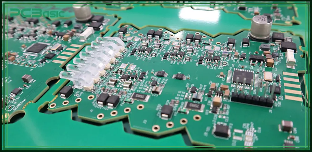
Ever had a board that passed visual inspection—but failed after reflow? Warpage is the invisible culprit. Here’s how to spot it early.
Place the PCB on a verified flat surface. A granite block works well. Shine a light from behind. If you see gaps, it’s warped. Simple, but effective for quick checks.
This tool measures small height differences. Move it across the PCB surface to track the curve. It's more accurate than visual checks. You’ll get a precise number, not just a guess.
Slide a feeler gauge between the PCB and the flat surface. Try different blades to find the exact gap. It’s low-tech, but surprisingly reliable—especially for quick checks on the shop floor.
Special jigs hold the board in place and help measure out-of-plane distortion. Often used in production QA. Good for consistent and repeatable checks.
Advanced systems use lasers or structured light to capture the entire surface profile. Very accurate, but costly. These are typically used in high-volume production environments.
Checking warpage isn’t about guessing. It’s about numbers. Standards matter.
Let’s talk numbers. The IPC-TM-650 2.4.22 standard outlines how to measure PCB warpage.
The method is simple:
1. Lay the PCB on a flat surface.
2. Use a height gauge or dial indicator to measure the highest deviation from the surface.
3. Divide that deviation by the diagonal length of the board.
That result? It’s your warpage percentage.
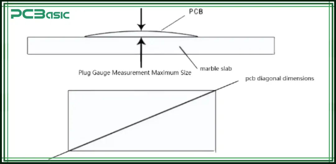
Warpage Calculation Formula (IPC-TM-650):
Warp (%) = (Maximum Deviation from Flatness / Diagonal Length) × 100
For example, a 0.5 mm bend on a 200 mm board equals 0.25%. That’s within limits.
But go over 0.75% for SMT boards—or 1.5% for through-hole—and you're in risky territory.
Why diagonal? Because warpage isn’t always straight. It can twist. Bend. Bow. The diagonal captures the worst-case scenario.
Want more precision? Use a coordinate measuring machine (CMM). Or a 3D scanner. These tools give a complete topography of the board surface. You’ll see the curve, not just a number.
Some high-end manufacturers even use thermal imaging. Why? To see how the board behaves when heated. Warpage during reflow can be worse than what you measure at room temp.
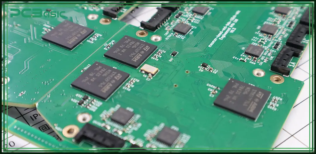
Fixing warped boards is tough. Prevention is better. So, how do you stop warpage before it starts?
Let’s look at proven methods.
Always design with symmetry in mind. Keep copper distribution even. Use the same number of layers above and below the center. Match dielectric thicknesses. Unbalanced layers can lead to unbalanced stress. And ultimately, warpage.
Use simulation tools to check balance early. Saves a lot of heartache later.
Avoid large copper pours on one side and not the other. That’s exactly how boards start to curl, even before reflow. Use dummy copper fills where needed. Keep thermal mass consistent. Some EDA tools can auto-balance copper. Use them.
Cheap FR4 bends fast. Especially under heat cycling. Use high-Tg or low-CTE materials if your application demands heat resistance. Polyimide boards are more stable under thermal stress.
Ask the manufacturer what materials they recommend for high-reliability boards.
Sudden heating causes stress. So does uneven heating. Set a proper reflow profile. Use gradual ramp-up and cool-down steps. Make sure the top and bottom zones are balanced.
Double-sided assemblies? Pre-bake the board. Or pre-reflow one side with low-temp solder paste.
Store boards flat, moisture-free, and at a controlled temperature. Use vacuum-sealed packaging if possible. Add desiccant packs. And always bake boards before assembly if they’ve been exposed to moisture.
Also, don’t stack boards without spacers. Weight from the top warps the bottom.
If the board is thin, large, or component-heavy—use fixtures. Reflow fixtures keep the board flat during soldering. They reduce mechanical stress and thermal sag.
It’s an extra cost. But it’s cheaper than scrapping 500 boards.
Sometimes, designers add too many layers or push tight tolerances just to squeeze in features. Ask yourself: is it worth it? More layers increase the design complexity. If not properly balanced, this leads to higher internal stress and warpage.
If the design allows, keep the layer count down. Use smaller boards. Go modular if possible.
Let’s put this in context. You build a 12-layer board for a medical device. Testing goes fine. But after the final reflow, some units fail. Pads are floating. X-ray shows bad solder joints.
The issue? Slight warpage—just 0.9%. But that’s enough to lift QFN corners and create open circuits.
Your yield drops by 15%. QA blames assembly. Assembly blames design. Now you’re reworking boards. Delays pile up. Customer confidence dips. All for 0.9%.
This happens in aerospace, too. Or EVs. Anywhere, reliability matters.
PCB warpage isn’t always visible. But its effects are loud—missed solder joints, machine errors, and field failures. What’s scary? It often goes unnoticed until it’s too late.
So, don’t wait for the issue to show up on the production floor. Start with design. Think about materials. Watch your copper balance. Bake your boards. Handle them right. And measure everything.
Because once the board bends—it’s hard to unbend. With the right processes, most warpage problems can be avoided. It’s not luck. It’s control. So next time your PCB looks flat, ask yourself: is it really?

Assembly Enquiry
Instant Quote
Phone contact

+86-755-27218592
In addition, we've prepared a Help Center. We recommend checking it before reaching out, as your question and its answer may already be clearly explained there.
Wechat Support

In addition, we've prepared a Help Center. We recommend checking it before reaching out, as your question and its answer may already be clearly explained there.
WhatsApp Support

In addition, we've prepared a Help Center. We recommend checking it before reaching out, as your question and its answer may already be clearly explained there.