Global high-mix volume high-speed PCBA manufacturer
9:00 -18:00, Mon. - Fri. (GMT+8)
9:00 -12:00, Sat. (GMT+8)
(Except Chinese public holidays)
Global high-mix volume high-speed PCBA manufacturer
9:00 -18:00, Mon. - Fri. (GMT+8)
9:00 -12:00, Sat. (GMT+8)
(Except Chinese public holidays)
HomePage > Blog > Knowledge Base > SMD VS NSMD: A Comprehnsive Comparison
NSMD pads are the non-solder mask defined that are not extended at the edges of their pads and the surface of copper is also exposed. Due to this exposed structure of the NSMD pads, soldering functions can be easily applied and the precision is also higher in quality. Also, the pad configuration will help strengthen the joints of solder and the volume of solder paste.
These pads are more precise and accurately used for specific tasks and applications during the manufacturing process. The mechanical strength in the solder joint is also a factor that emphasizes the fine-pitch BGA and it reduces the bridges of forming solder.
There are two types of designs in the Printed Circuit Board (PCB): NSMD and SMD pads. The comparison between both pads is based on their performance, usage, structure of design, and the durability of central PCB design and applications. If your application needs the rise time, pulse shaping, and non-optimal features, then NSMD pads are the best choice due to the sliced bread.
Another scenario is that if you do not require the complex structure of design for your applications, then the SMD choice will be better at this stage. However, SMD pads are often used in high-precision and high-density applications in the PCB structures. These pads have the function of great mechanical flexibility and solder joint reliability and are also simply designed like that BGA.

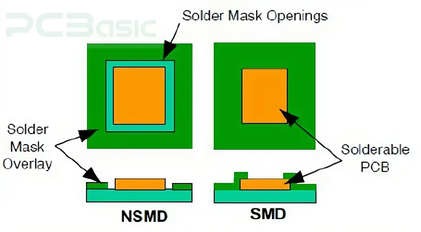
The definition of a Solder Mask Defined, abbreviated as the SMD pads, is copper pad layouts with the protection of a solder mask. The pad profile cross-section dimensions are determined by the solder mask applied to the layout. These pads are applied in PCBs for the performing of different functions.
The most beneficial factor in the application of SMD pads is providing maximum degree control while soldering functions. The soldering mask minimizes the risk of the spread of solder and also provides the best connections for the components. There are some advantages for the SMD pads in the following:
· Improved the solder mask with adhesion and joint formation is reliable;
· Reduced the solder wicking that helps in the minimization of the volume of solder.
SMD pads have many advantages as discussed. Therefore, there are also some drawbacks in the list that deserve attention while applying them.
· Limited pad size of solder mask and components cannot be used properly;
· Having potential for solder joint cracking due to the thickness of the solder mask.

The definition of a Non-Solder Mask Defined abbreviated as NSMD pads, differs from the SMD pads due to the copper pad is not covered by the solder mask in any conditions. Therefore, here is the space often called the solder mask gap between the copper pad perimeter and the solder mask. The design of NSMD pads has more flexibility and placement in the reliable terms.
There are features in the NSMD pads in which the configuration has some beneficial terms in comparison to the SMD pads. These advantages are the following:
Greater pad flexibility: The design of the pad is more flexible due to the absence of a solder mask in the outline of the pad, as the technician can alter the shape and size according to their demands.
Improved solder joint reliability: In the NSMD pads, the solder joint reliability is improved due to the greater pad flexibility. Having the pad flexibility is the advantage of reducing the cracking of solder joints and also providing more mechanical stress tolerance.
Larger copper surface area: These pads have more copper area that emphasizes the solder joint strength and stress management for the NSMD pads in the applications.
Although the NSMD pads have many advantages, on the other hand they also have drawbacks. Some issues can cause difficulties while performing the PCB design by using NSMS pads. Some of the disadvantages are below:
Less control over solder volume: always having less control over solder volume due to the absence of a solder mask around the pad area. It can cause a difference in the solder volume of the pad and undesirable creation of a bridge of pads.
Higher production costs: In comparison to the PCBs, the NSMD pads have higher production costs due to the alignment of the solder mask and the precise dimensions of pad size and geometry.

The Solder Mask Defined SMD and Non-solder Mask Defined have major differences in pad designs and the configuration of the Solder mask application to the pads. In the SMD pads, the solder mask also covers the copper parts, but in the NSMD pad, the copper parts are not covered by the solder mask.
Therefore, the NSMD pads are more reliable and effective as compared to the SMD pads due to the solder mask difference. In terms of mechanical stress factor, the SMD is more worthy than NSMD due to the pad design thickness in the SMD.
The NSMD pad has a more flexible quality than the SMD due to the solder mask design of the pad, and it also helps design the BGA applications. The shape and size selection based on wave soldering is applied.
SMD pads can deal with the applications of high-density properties and special-purpose control for soldering where it is needed. In an SMD pad, there is no chance of spreading the solder mask over the whole area, and it enables the characteristics of neat and good connections of components.
Both types of pads are affecting the process of soldering applications. Therefore, NSMD pads have the formation of solder joints in terms of flexibility, but it can cause loss of control volume of the solder mask in the pad.
|
Parameters |
SMD Footprint |
NSMD Footprint |
|
Mask opening vs. Pad |
Solder mask whole covers pad edges |
Solder mask more clear of pad edges |
|
Solder volume control |
Better control of solder volume |
Reduce control of solder volume |
|
Pad shape |
Typically square or rectangular |
Can be more flexible in shape and size |
|
Bridging risk |
Less due to restricted solder spreading |
High due to greater solder spread |
|
Registration needs |
High mask registration tolerance needs |
Less mask registration requirements |
|
Solder voiding |
Lower prone to voiding |
Highly prone to voiding |
|
Design and assembly cost |
Lower cost due to simpler design |
Typically higher due to complexity |
There is a dependency upon the choice of the application of your PCB design as well as the BGA nature of your design. The differentiation of NSMD and SMD pads is clearly described in the whole article. In the comparison scenario, NSMD pads have more design flexibility and more reliability in the structure of mechanical strength, and also provide the BGA applications for different sizes and shapes according to our applications.

Assembly Enquiry
Instant Quote
Phone contact

+86-755-27218592
In addition, we've prepared a Help Center. We recommend checking it before reaching out, as your question and its answer may already be clearly explained there.
Wechat Support

In addition, we've prepared a Help Center. We recommend checking it before reaching out, as your question and its answer may already be clearly explained there.
WhatsApp Support

In addition, we've prepared a Help Center. We recommend checking it before reaching out, as your question and its answer may already be clearly explained there.