Global high-mix volume high-speed PCBA manufacturer
9:00 -18:00, Mon. - Fri. (GMT+8)
9:00 -12:00, Sat. (GMT+8)
(Except Chinese public holidays)
Global high-mix volume high-speed PCBA manufacturer
9:00 -18:00, Mon. - Fri. (GMT+8)
9:00 -12:00, Sat. (GMT+8)
(Except Chinese public holidays)
HomePage > Blog > Knowledge Base > What Are PCB Test Points (circuit board test points)?
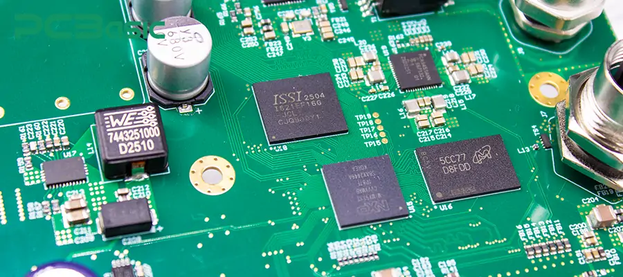
Electronic gadgets in simple forms, like smartphones, to complex ones, like industrial machines, all need to house PCBs operating glitch-free. That's where the test points for a circuit board come into the picture. All boards go under strict testing before they finally make it into products. With test points on PCBs, the monitoring and measurement of electrical properties both at production and post-production are accessed easily.

The access points are located in places so that problems brought about by faulty connections or wrong component values can be traced. Circuits are becoming more complex, and components are becoming smaller. Thus, circuit board test points play an essential role in product reliability. They know why it is the key for professionals to improve the quality of their products and reduce defects in the market.
In a PCB's life cycle, such test points have many essential roles during design and fabrication. Here are some of the crucial roles of test points on a printed circuit board:
Some of the primary uses are checking electrical integrity with test points on a PCB. This is done by ensuring that paths are continuous without any fault in unwanted shorts or open circuits in the PCB. Examining these test points will tell in no time whether all these connections are intact and working according to your specifications. This step prevents an entire PCB from general electrical failures, rendering it useless.
In addition to giving a general test for the electrical integrity of the PCB, test points exercise a lot of different components on the board individually. Nearly every element on the board, whether a resistor, capacitor, or integrated circuit, has specific parameters within which it must operate for the entire board to function as intended. Test points allow engineers to measure such components in isolation without interfering with the rest of the circuit.
Other uses of test points are during design verification: a PCB design must be tested against all specifications before it is put into production. The test points offer a location where the engineers can measure and validate the performance of various sections of the circuitry to reach design-specified performance under different operating conditions. That way, expensive mistakes will not appear.
Of course, something can still go wrong with a PCB, even after the production stage, either at the assembly and test stages or in the field. In this case, the test points become vital for troubleshooting and debugging. If anything goes terrible at this point, an engineer can probe around the circuit using the test points and quickly tell where things went wrong. This diagnosis and quick fixation of issues is necessary to stay on course regarding the production timeline, with quality assured in the final product.
When considering high-speed or high-frequency PCBs, one needs to maintain signal integrity. Generally, test points are applied for signal integrity monitoring since they offer access to the crucial nodes of the circuit. An engineer will be able to measure the signal characteristics using measurement points, such as voltage levels, timing, and noise, to stay within tolerable limits. This is especially significant in applications where signal failure corrupts the data or makes the system fail.

It is not only a manufacturing requirement but also a technical requirement, including test points in any PCB design. It helps access appreciable value and makes the whole testing process easier, efficient, and smoother. A design without test points renders this process of identification and diagnosis especially difficult, which can lead to delays and inflated production costs.
Test points in a PCB are vital during manufacturing. Every PCB must be checked to determine whether it meets the specifications before it goes into the next step of production. It helps in fault prevention since an engineer can easily reach some parts of the circuit for testing. Therefore, only quality boards make their way into the final products.
On the contrary, these test points make it possible to detect any failure of the manufacturing process at an early stage in the life cycle of the PCB. The availability of test points during a product's manufacture serves to find problems well before they arise and spiral into costs that are too high to consider. Such means of quality assurance stand a good chance of improving final product reliability, hence diminishing the chances of costly recalls or repairs in late life.
In fact, most of the benefits from allowing test points on the PCB accrue to efficient manufacturing and high product quality, thus enhancing customer satisfaction.
Reduced time: the test point provides the shortest path to the necessary area; hence, testing can be much quicker, making very high-volume manufacturing possible.
Better fault detection assurance: faults will be detected and diagnosed in time by ensuring only quality boards reach the final assembly.
Debugging is better: The test points make debugging easy. They may be easily performed in less time. Thus, the problems may be solved at the time of manufacturing and after the manufacturing time.
Quality Testing at Lower Costs: Such a framework can back up exhaustive testing to ensure complete avoidance of expensive rework, reducing the chances of defects in the market.
Automated Test: Automatically inserts test points and allows for high-throughput production of repetitive and repeatable testing procedures.

These days, there are various types of test points that suit different purposes. Knowledge of the test points may help make the right choice to suit one's needs for a particular purpose.
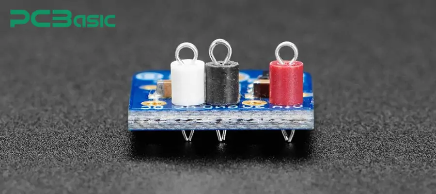
Such a device has seen more applications in manual testing and debugging and has taken the form of the test point-probe test point. For instance, it is nothing more than an unshielded area of a printed circuit board where a test probe must be placed to measure an electrical signal. It is easily performed, and one has direct access to part of the circuit during testing. Alternatively, they can be simple in design and, hence, unsuitable for automated testing.
These are component packages designed to be mounted on the surface of printed circuit boards. Their finer and smaller size compared to all other types of standard probe test points makes them suitable for high-density circuit boards. SMT test points are used explicitly in automated test environments as they can be probed by automatic test equipment with reasonable accuracy.
Auto-test points are probe test points for high usage by ATEs. They may have more robust construction than the average probe test point since they undergo so much probing in high-volume manufacturing. Often, the auto-test points are sprinkled where the test equipment can reach them easily, thus allowing for efficient and repeatable testing from board to board.
Through-hole test points are mainly applied on printed circuit boards with through-hole components. These test points occur out of plated holes traversing a PCB and providing access to the electrical connections on either side of the board. In most cases, applications find their way into these test points to extend the comprehensive test coverage of a whole PCB.
Planning and strategic placement of PCB are required for effective testing by test points at the design stage. One can be sure that an engineer placed test points effectively for a practical test by speedily following best practices.
The testing equipment may easily access whatever test points are placed on the PCB. The test points must be kept where they don't interfere with other elements or mechanical fixtures. This access must be accessible in automated tests, so the testing equipment reaches the test point without interference.
High signal integrity is a big concern in high-frequency circuits. Test points should be placed to minimize the risk of interference with a signal that may lower the accuracy of the test results or circuit performance. Adequately planned test point placement by the engineer along the high-speed signal path reduces the possibility of adding additional capacitance and inductance to the circuit.
Space is a general issue in a high-density populated PCB, and one must compromise between the test points one needs and space. The positions of test points can be selected in a manner that could serve the test point with its importance at that position and where it would not compromise too much on the PCB design. This may result in engineers sometimes having to trade off test points against available board space and trying to hit the most sensitive areas.
Proper documentation and labeling make the test points traceable for possible testing. All the test points on the PCB should be labeled in the design documentation along with a note of its function and the signal to be tested. This is very important at the time of large volume manufacturing when teams for testing may vary.
 About PCBasic
Time is money in your projects – and PCBasic gets it. PCBasic is a PCB assembly company that delivers fast, flawless results every time. Our comprehensive PCB assembly services include expert engineering support at every step, ensuring top quality in every board. As a leading PCB assembly manufacturer, we provide a one-stop solution that streamlines your supply chain. Partner with our advanced PCB prototype factory for quick turnarounds and superior results you can trust.
A test point on a PCB allows access to test and verify at each stage of manufacture. Hence, placement of the PCB test points at this phase in a printed circuit board design provides a vision for products coming off the production lines, meeting quality and reliability standards.
These test points will facilitate the testing work and reduce costs due to better product performance. Since electronics have more refined devices, the role of PCB test points in the success of such devices will be paramount.
Such assumptions imply good practice in the placement and utilization of test points so that the engineers may work out their designs accordingly for efficiency and dependability toward successful and reliable electronic products.
1. Why are the test points applied in a PCB circuit?
Some of the test points applicable to a PCB circuit are used to easily access signals or power lines. Testing confirms that the circuit's functionality and integrity are okay without damage to components.
2. How would you probe test points located within the PCB?
Testing is done using probes at marked test points on a PCB. Voltage, current, and signal integrity can be measured at different points in the circuit.
3. In manufacturing, what purpose are test points used on a circuit board?
Circuit board test points are essential for manufacturing the product to perform functional testing of a PCB, hence enabling the early detection of faults that can help maintain the quality standards of the final product.
4. SMT test points—what are they, and how does each differ?
SMT test points are small, flat pads for testing surface-mounted components. The main difference from traditional test points is that they address the recently developed SMT components.
5. Where on the PCB should I pick a test point location?
Test points of the design strategy should be located on the PCB so that all critical signals inside it are easily accessible. The layout must consider where exactly that signal will travel and at what locations tests will most likely be needed.

Assembly Enquiry
Instant Quote
Phone contact

+86-755-27218592
In addition, we've prepared a Help Center. We recommend checking it before reaching out, as your question and its answer may already be clearly explained there.
Wechat Support

In addition, we've prepared a Help Center. We recommend checking it before reaching out, as your question and its answer may already be clearly explained there.
WhatsApp Support

In addition, we've prepared a Help Center. We recommend checking it before reaching out, as your question and its answer may already be clearly explained there.