|
Term
|
Full Name
|
Meaning
|
|
PCB
|
Printed Circuit Board
|
A board that supports and connects electronic components using conductive pathways, tracks, or signal traces etched from copper sheets laminated onto a non-conductive substrate.
|
What is PCB?
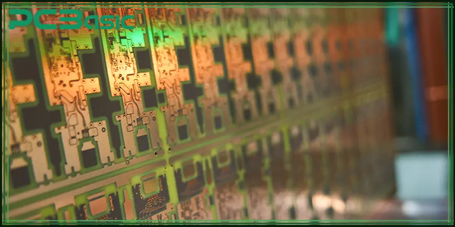
In modern electronics, a Printed Circuit Board (PCB) is one of the essential components of the device. PCBs are the fundamental building blocks of modern technology, acting as the infrastructure that supports and interconnects electronic hardware components. Additionally, a printed circuit board (PCB) is a common component in everything from consumer electronics to aerospace and medical devices.
Moreover, PCBs were designed to supersede the conventional wire-to-wire connections made through harnesses — providing a method to assemble electronic circuits that could be far more compact, reliable, and efficient. They are created by etching or printing conductive routes on an insulating substrate, like fiberglass or plastic, enabling the flow of electricity between components.
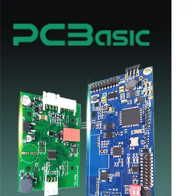 About PCBasic
Time is money in your projects – and PCBasic gets it. PCBasic is a PCB assembly company that delivers fast, flawless results every time. Our comprehensive PCB assembly services include expert engineering support at every step, ensuring top quality in every board. As a leading PCB assembly manufacturer, we provide a one-stop solution that streamlines your supply chain. Partner with our advanced PCB prototype factory for quick turnarounds and superior results you can trust.
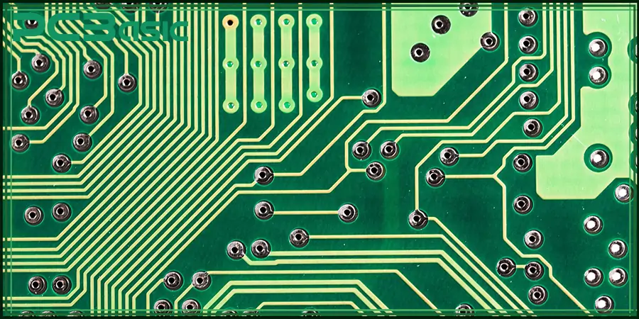
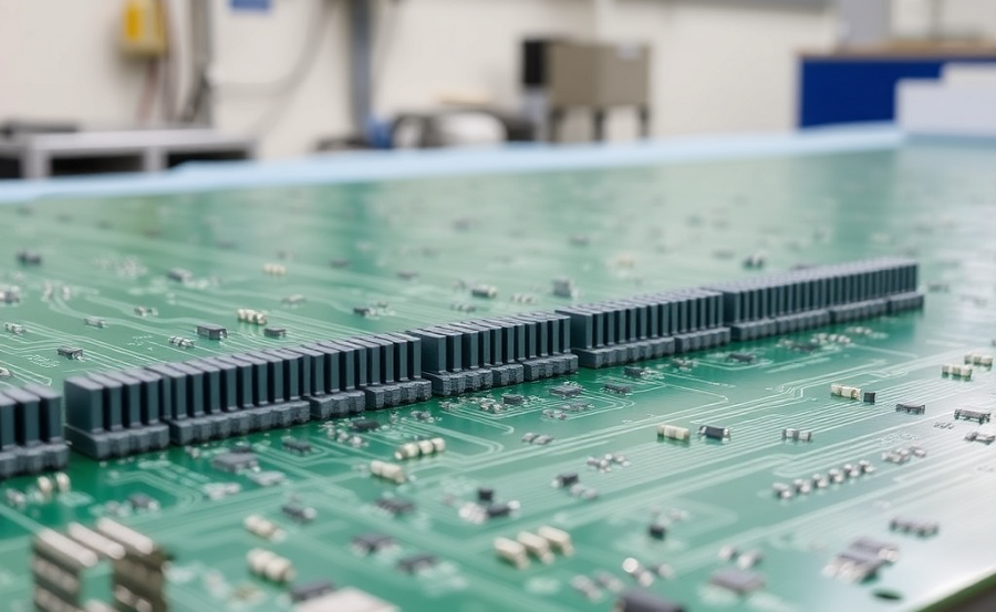
PCB Components
A PCB has the following main elements:
· Base Material: Most commonly fiberglass or plastic, that provides structural support.
· Copper Layers: A copper foil portion is laminated onto the substrate in thin layers to form the conductive pathways.
· Solder Mask: A robust layer that is coated over the copper to preclude short circuits and oxidation.
· Silkscreen: A layer used to print labels, logos, or component identifiers on the PCB.
· Electronic Component: Integrated circuits (ICs), resistors, semiconductors, etc. are on the board.
PCB Layers
PCBs comprise various layers that support functionality, durability, and performance. PCB Layers Overview PCB layers can be categorized as follows:
Base Material (Substrate Layer)
FR4 (fiberglass-reinforced epoxy) generally constitutes the PCB's base. It gives mechanical strength and insulation.
Applications:
· Used in all PCBs as a foundation layer.
Advantages:
· Long lasting.
· Electrical insulating.
· Heat resistant.
Disadvantages:
· Varies in cost.
· Thermal performance.
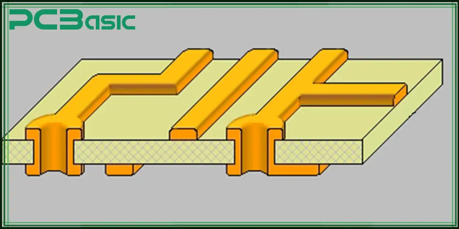
Copper Foils (Conductive Traces)
It’s thin sheets of copper pressed onto a substrate. The traces are etched to allow the electrical current to flow. Commonly seen in single-layer, double layer and multi-layer PCBs.
Application:
· Used in all types of PCBs for passing on the electric signals between components.
Advantages:
· Great conductivity.
· Good for high data rate signals.
· Power capable.
Disadvantages:
· Increases cost.
· Increases complexity of manufacturing.
Signal Layers
Layers whose purpose is to transfer electrical signals between components. A multi-layer PCB comprises many signal layers stacked one above the other for complexity in the circuit.
Applications:
· Used in multi-layer PCBs to route signals in high-density designs (i.e., processors, GPUs).
Advantages:
· Minimizes the interferences on the signal.
· Permits a complex route.
· Improves the functionality of PCB.
Disadvantages:
· Increased PCB complexity.
· Designed very carefully to avoid crosstalk.
Power Plane & Ground Plane
Power Plane: A layer of thick copper that distributes power (VCC) across the PCB.
Ground Plane: A copper layer that gives a return path to the current (the ground).
Applications:
· Used in multilayer printed circuit boards for high-speed electronics for stable power distribution.
Advantages:
· Minimized electrical noise.
· Increased signal integrity.
· Ensures reliable power delivery.
Disadvantages:
· Increases complexity and manufacturing cost.
Insulating Material (Dielectric Layer)
Insulating material keeps conductive layers apart to avoid shorting. It is composed of materials such as prepreg (pre-impregnated fiberglass).
Applications:
· Used in all PCBs to insulate the conductive layers and to avoid short circuits.
Advantages:
· Insulates and minimizes interference.
· Enhances thermal stability.
Disadvantages:
· Not all materials have the same dielectric constant which affects signal performance
Solder Mask Layers
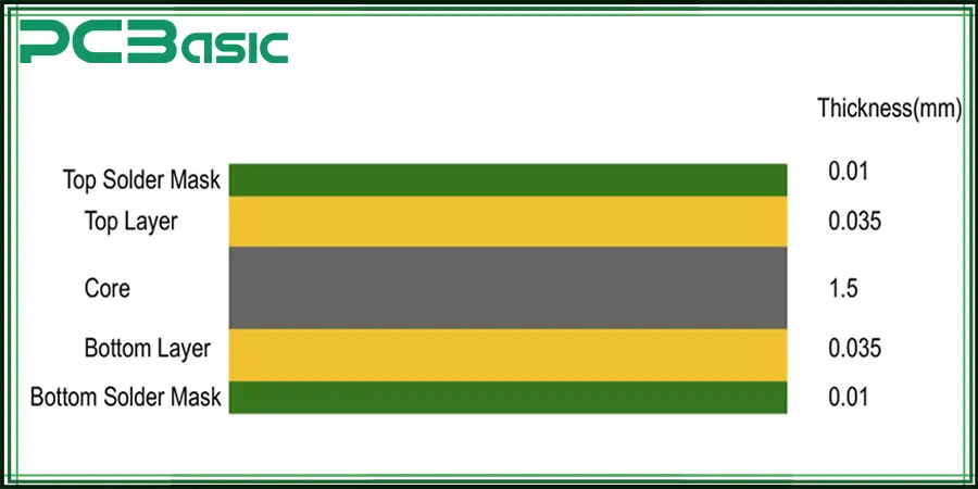
It is a protective coating covering the copper traces. It is usually green, blue or red. This layer helps avoid oxidation and unwanted solder bridges.
Applications:
· Used in all PCBs to cover copper traces and avoid solder bridging.
Advantages:
· Protects from oxidation.
· Increases durability.
· Provides better contact for soldering.
Disadvantages:
· Requires precision in application.
· Improper masking can create defects in manufacturing.
Silkscreen Layer
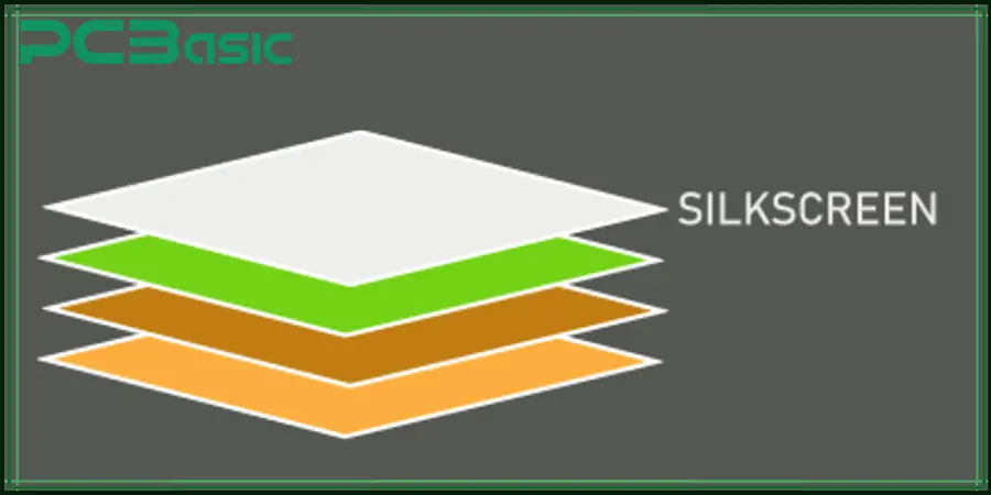
It is text on paper or symbols (namely component labels, logos, reference indicators). Silkscreen layer helps assists with assembly and debugging.
Applications:
· Used in all PCBs for component, logo, and reference indicator labels.
Advantages:
· Helps with assembly, debugging, and documentation.
Disadvantages:
· Limited in marking size.
· Requires a professional approach for high-density PCBs.
Solder Paste Layers (For SMT Assembly)
It is used during Surface Mount Technology (SMT) assembly. Solder paste is included for attaching components.
Applications:
· Used in Surface Mount Technology (SMT) PCBs for placing components.
Advantages:
· Secure electrical connections.
· Increases precision during automated assembly.
Disadvantages:
· Stencil printing is needed, and improper paste application can lead to defects.
Keep-Out Layer
The keep-Out layer designates forbidden zones where components or traces should not be placed. It ensures adequate spacing and prevents manufacturing quality issues.
Applications:
· Limits what to place in which area in PCB design components or traces.
Advantages:
· Helps keep the layout from becoming congested, the manufacturability and spacing are correct.
Disadvantages:
· Restricts design flexibility (demands careful planning).
Types of PCB Based on Layers
Single-Layer PCB:
A Single-Layer PCB has a single conductive layer (most commonly copper) on a non-conductive substrate (most often FR4, phenolic, or paper-reinforced epoxy). Copper traces are used to create the electrical connections on the board, which are then coated with a solder mask to protect against oxidation. Simple electronic devices mainly use this type of PCB to manufacture low-cost.
It has only one layer. That layer can be of:
· Substrate Layer (Base Material): The composition is normally FR4, phenolic resin, or epoxy
· Conductive Layer: A thin layer of copper for circuit pathways.
· Solder Mask: Prevents traces from short-circuiting and corrosion.
· Silkscreen: To identify what components are on the board.
Applications:
· Calculators.
· Power supplies.
Double-Layer PCB
A Double-Layer PCB contains copper conductive material on both PCB sides. Vias (plated through-holes) provide electrical interconnections between layers, allowing for more compact circuits. This type of PCB is a bit more versatile than single-layer types and accommodates moderately complex circuitry.
Applications:
· Industrial Controls
· Automotive Electronics
· Smartphones & Audio Devices
It has two layers. Those layers can be:
· Substrate Layer: FR4 or epoxy resin.
· Bottom Copper Layer: The conductive paths for circuits.
· Top Copper Layer: Additional circuitry for higher complexity.
· Vias: Were used to make electrical connections between the top and bottom layers.
Multi-Layer PCB
A Multi-Layer PCB is a layer of three or even more punched out conductive layers placed on top of each other with dielectric layers of insulation between each of them. For example, high speed, compact structure is used in the military, computers, communication and other equipment.
Applications:
· Smartphones & Computers
· Medical Equipment
· Defence Space & Security
· Telecommunications at High Speed
Multi-Layer has 4+ layers. Those layers can be:
· Cores Substrate: Structural strength
· Copper Layers: To achieve circuit complexity, several conductive layers
· Isolation layer: Sits between conductive layers.
· Power & Ground Planes: Minimize signal interference and carry power.
· Solder Mask & Silkscreen Layers: Protection and identification.

Flexible PCB:
Flexible PCBs are comprised of flexible materials (commonly polyimide (PI) or polyester (PET)) which can bend, twist, or fold without breaking. These are extensively used in wearable devices, automotive electronics, and Aerospace applications.
Applications:
· Smartphone & Wearable Devices.
· Automotive Dashboards.
· Medical Devices.
· Spacecraft & Satellites.
Flexible PCB’s layers vary board to board. Those Layers can be:
· Flexible Substrate (Polyimide or PET).
· Copper Conductive Layer.
· Adhesive Layer.
· Coverlay, protective.
· Silk Screened for components.
Rigid PCB
A Rigid-Flex PCB is a type of PCB that combines delta rigid and flexible sections in a single board. It is used in small devices with restricted volume such as military devices, cameras, and medical implants.
Applications:
· Healthcare MID (Medical Devices (pacemakers, hearing aids).
· Cameras & Wearable Tech.
· Industrial Control Systems.
Layers in Rigid-Flex PCB:
· Rigid Sections (FR4 Material)
· Innovations For Flexible Sections (Polyimide Substrate)
· Copper Conductive Layers
· Prepreg & Adhesive Layers
· Flex Sections: Protective Coating
High-Frequency PCB:
A High-Frequency PCB is capable of working at frequencies above 1 GHz with the help of low-loss materials, such as PTFE (Teflon) and Rogers laminates. This is very important aspect of RF (Radio Frequency) and microwave applications.
Applications:
· 5G Base Stations.
· Radar & GPS Systems.
· Satellite Communication.
· High-Speed Data Processing.
Layers in High-Frequency PCB:
· PTFE or Rogers Substrate.
· Copper Conductive Layers.
· Dielectric Insulating Layers.
· Power & Ground Planes.
· Solder Mask & Silkscreen.
HDI PCB
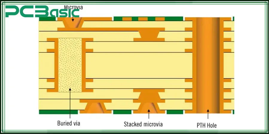
HDI PCB (+High-Density Interconnect PCB) is a type of printed circuit board that has a high density of pads, traces, and vias. It employs microvias, blind and buried vias, and fine trace widths to enable miniaturization and high-speed signal transmission. These HDI PCBs are vital for small form-factor electronic devices such as smartphones, laptops, and state-of-the-art medical instrumentation.
Applications:
· Smartphones & Tablets
· Laptops & Wearable Tech
· Medical Devices
· Automotive Electronics, ADAS (Advanced Driver Assistance Systems).
· Aerospace & Military: Applications in satellites, avionics, and defense systems.
· High-Speed Computing
· IoT Devices & Equipment for 5G Enterprise
Some include HDI PCBs that can have different layers depending on the design requirement. The typical layers include:
· Core Substrate: Main layer material, usually FR4, PTFE, or Rogers laminate.
· Copper Layers: Several conductive layers are used for power, ground and signal routing
· Microvias (Laser Drilled Vias): Vias interconnect differing layers effectively.
· Dielectric Layers: Insulating layers interposed between conductive Signal traces.
· Prepreg Layers: Put adhesive material between layers to bond them.
· Power & Ground Planes: Provide stable power and reduce noise.
· Solder Mask & Silkscreen: as the need to protect & label the components.
Structure of HDI PCB Types:
· 1+N+1 (Single HDI Layer): one HDI layer on both sides
· 2+N+2 (Double HDI Layer): Two HDI layers on all sides.
· Any-Layer HDI: Microvias connect any layer for ultimate design flexibility.
PCB vs. PCBA

|
Features
|
PCB
|
PCBA
|
|
Definition
|
A bare board without components.
|
An assembled PCB with soldered devices.
|
|
Functionality
|
Non-functional.
|
Operational electronic circuit.
|
|
Manufacturing
|
Etching, drilling, lamination.
|
Placement of components, soldering (SMT/THT).
|
|
Testing
|
Checks for continuity/shorts.
|
Functional and performance testing.
|
Key Differences
· PCB is just a board, while PCBA is an operation-ready electronic module.
· PCBs are passive structures, while PCBAs incorporate active components such as microcontrollers, resistors, capacitors, and ICs.
· PCB is the main component of the PCBA process while PCBA emphasizes the assembly and function of circuits, while PCB is the fabrication of the board itself.
· Testing the PCBA is more expensive, because it verifies the operational performance of the circuit board, while PCB testing only checks for continuity and board structure defects.
PCBasic's PCBA Services
We provide PCB assembly (PCBA) one-stop service, including:
Prototyping & Low-Volume Production.
PCB Design & Manufacture at High Speeds.
Automated SMT and Through-Hole Assembly.
Rigid & Flex & Rigid-Flex PCBs.
Quality Assurance (AOI, X-Ray, Functional Testing, Flying Probe Testing...).
Conclusion
PCB and PCB layers along the types of PCB are crucial for electronics design. The stacks of boards in multi-layer PCBs can be daunting, but each layer (copper, substrate, solder mask, silkscreen, etc.) has its own part to play in the functionality of the device.
Through quality design, selection of proper materials, and adherence to testing standards, engineers can enhance the reliability and lifetime of the PCB.For engineers, knowing a PCB's materials, layer structures and design best practices is vital to ensure that their electronics will be longlasting and high-performing. Even hobbyists and students can make their projects come alive, using inexpensive PCB design software.
With new technologies, such as IoT, AI hardware, and wearable technology, demand for PCBs will never fade. Whether you are repairing a defective board or deploying a new revolutionary device, familiarity with PCB fundamentals can help you succeed in the consistently-escalating electronic domain.