Global high-mix volume high-speed PCBA manufacturer
9:00 -18:00, Mon. - Fri. (GMT+8)
9:00 -12:00, Sat. (GMT+8)
(Except Chinese public holidays)
Global high-mix volume high-speed PCBA manufacturer
9:00 -18:00, Mon. - Fri. (GMT+8)
9:00 -12:00, Sat. (GMT+8)
(Except Chinese public holidays)
HomePage > Blog > Knowledge Base > PCB DFM | PCB Design for Manufacturability
Designing a PCB is the easy part. Getting it manufactured correctly? That’s where things often fall apart. You can spend days crafting the perfect layout. But if you ignore the manufacturing process, your design won’t make it past the fabrication stage. Or worse—it gets built wrong.
That’s why PCB DFM, or PCB design for manufacturability, is a big deal. It's not an afterthought. It's a mindset. One that ensures your PCB is not just functional but also physically manufacturable—without delays, errors, or surprises.
Let’s dig into what DFM actually means for PCB design, and why every serious hardware engineer needs to get this right.
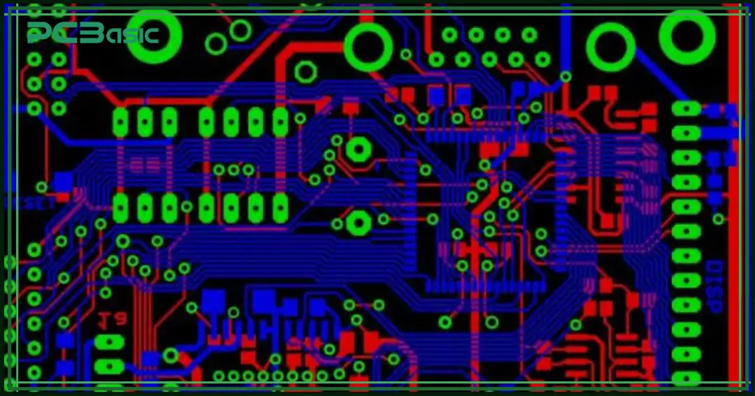
DFM (Design for Manufacturability) means exactly what it sounds like. It’s designed with the manufacturing process in mind.
In PCB design, that includes the entire lifecycle—from fabrication to assembly. You are not just thinking about traces and nets. You are thinking about:
• How small can the manufacturer reliably drill?
• What copper weight do they use?
• Will your solder mask align correctly?
• How does the board get depanelized?
• And if the components can actually be placed and soldered?
DFM is about removing friction between the designer and the factory floor. It prevents errors before they happen. And no—your EDA tool won’t automatically handle this for you. That’s a myth.
You have to actively apply DFM rules and constraints during layout. You need to match your design choices to the capabilities of your fabrication and assembly vendors. If you fail to do that, you might get a phone call you don't want.

Let’s be blunt: DFM can make or break a hardware project. You could have a fully simulated, error-free schematic. A layout that passes every ERC and DRC check. Yet your board still fails during production.
Why? Because the design wasn’t optimized for real-world manufacturing. Here’s what can happen without proper DFM:
• The board gets rejected by the manufacturer to trace width violations.
• Drill files don’t match the manufacturer’s tooling.
• Component placements are unbuildable due to spacing or orientation.
• Poor solder mask alignment leads to shorts.
• Via structures are not supported by the manufacturer's stack-up.
Every small issue adds up. More time. More risk. Sometimes even a full board re-spin. This isn’t some theoretical warning. In 2023, more than half of PCB delays came down to DFM mistakes that could have been avoided.
Skipping DFM guidelines doesn't save time. It costs you. Here's what usually happens:
• You pay rush fees to patch last-minute issues.
• Your engineers waste hours troubleshooting.
• You miss deadlines that mattered.
• Your contract manufacturer loses confidence in your team.
But it does not have to go that way. Engineers who build with DFM in mind get their boards out faster, cheaper, and more reliably. It's not hype. It's an edge most teams overlook.
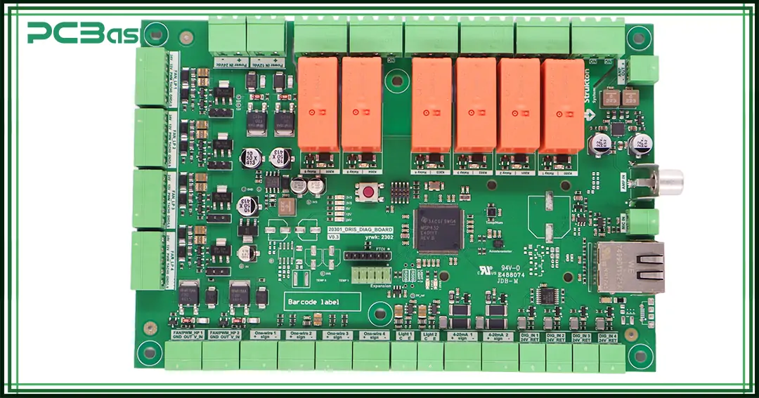
So, where should you focus during the layout? These are the key areas that make or break manufacturability:
Every PCB manufacturer has a minimum trace width and minimum copper spacing. These depend on copper thickness, etching process, and board complexity. If your traces are too thin, they might get over-etched. If your spacing is too tight, you risk shorts.
Your routing must align with the fabrication requirements. Some fabricators offer 4/4 mil (trace/space), while others need 6/6 or more. Always check. Use a trace width calculator to size traces properly for the current flow. IPC-2152 is a good standard to follow.
Not all vias are created equal.
You’ve got:
• Through-hole vias
• Blind and buried vias
• Microvias (for HDI designs)
Each comes with specific fabrication constraints. You can't just use tiny microvias and expect every manufacturer to support them.
DFM means knowing your via types, their tolerances, and the minimum drill-to-copper clearance required. Also, avoid using a via-in-pad unless necessary—it adds cost and complexity during assembly.
Pads must be sized based on both component package and plating tolerances. A via or hole without a proper annular ring is a structural risk. The ring ensures electrical and mechanical connection.
IPC recommends at least 0.15 mm (6 mil) for the annular ring. Your manufacturer might ask for more, depending on drill accuracy. This is especially critical for vias and press-fit connectors.
Solder mask defines the non-conductive layer that covers your board, leaving openings for pads and vias. Problems happen when:
• The mask opening is too small and covers the pad.
• Or too large and exposes too much copper.
Both lead to poor solder joints or shorts. Also, the solder paste layer must align with the pad. If your stencil openings don’t match the footprint, you’ll have cold joints or tombstones during reflow.
Use mask expansion settings carefully. Standard values are 4–6 mil, but always check with your manufacturer.
DFM also means placing components where they can be built and soldered. You need to:
• Avoid placing parts too close to board edges.
• Leave space for pick-and-place machines to operate.
• Follow orientation guidelines for QFNs, BGAs, and polarized parts.
• Respect thermal and mechanical clearance.
A tight layout might work electrically. But if your CM can’t place or reflow the parts correctly, it’s a failure.

Skipping DFM is like building a house without checking if the doors fit. Everything might look great in the CAD view. But when it hits the manufacturer's floor, issues pile up.
Here are some of the most common yet costly DFM mistakes engineers still make:
Every manufacturer shop has a process window. Minimum spacing. Minimum drill size. Copper-to-board edge clearance. When you ignore these specs, you force the manufacturer to either:
• Reject the board.
• Tweak it themselves (which you won’t like).
• Or worse, manufacture it with defects.
Trace width too small? It could cause over-etching or open circuits. Hole sizes off-spec? Expect low plating quality. These are basic DFM rule violations, and yet they happen all the time.
Multilayer boards are powerful—but risky if not designed right. Blind and buried vias, via-in-pad designs, and microvias all sound cool on paper. However, not every fabricator can build them. And if they can, it’s going to cost you.
If your layer stack isn't defined properly with realistic material specs and dielectric values, you may end up redesigning the entire thing. Always cross-check the manufacturer's capabilities before you finalize the stack.
The annular ring is the copper pad surrounding a drilled hole. If the ring is too narrow, it becomes a yield problem. Especially in vias or through-hole pads.
A via that barely holds copper around the hole will crack under stress. Or even during reflow. IPC standards recommend minimum values, but it’s better to leave margin.
Yes, it’s a simple one. But it still causes real trouble. Text on solder pads burns off and leaves residue. Component IDs printed under parts are completely useless. And cluttered silk layers confuse the assembly technicians. Proper DFM includes silkscreen checks as standard.
If your board does not include tooling holes, fiducials, or breakaway tabs, your assembler has to improvise. That never ends well.
You must design for panelization. That includes leaving spacing between units, handling rails, and considering how the boards will be separated. Skipping this step adds time and cost later.
If you don’t provide test points for essential signals, how will your QA team check continuity? Or power rails? Or key signals?
Design for test (DFT) overlaps with DFM. Every well-thought-out PCB should include proper probe-friendly pads or via access for functional testing.
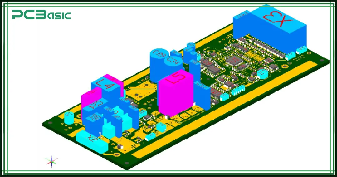
So now you know the risks. Let’s flip it—how do you actually apply DFM during real-world PCB development? Here’s a practical flow that many professional design teams use:
Before you start layout, lock in who’s going to manufacture your boards. Every shop has its own process tolerances. Don’t design blind. Get their DFM guidelines, stackup templates, and via capabilities upfront.
Ask for:
• Drill tables
• Copper thickness options
• Minimum spacing
• Layer stack examples
• Solder mask and silkscreen requirements
This saves hours of guessing and rework later.
Modern EDA tools like Altium, KiCad, and OrCAD let you build design rules into the project itself.
Set clear:
• Clearance rules
• Drill size limits
• Trace width tables (based on current)
• Annular ring minimums
• Solder mask expansion
Doing this from the start helps you catch DFM errors while designing, not after.
Avoid DIY footprints unless you're 100% sure. Use libraries that follow IPC-7351 or are validated by your CM (contract manufacturer).
Ensure:
• Pad sizes are within spec
• Thermal reliefs are added where needed
• Polarity and pin 1 indicators are correct
• Courtyard and keep-out areas are included
Bad footprints are a silent killer. Many DFM issues begin here.
This step is non-negotiable. Before you send your files to the manufacturer, run a full DFM analysis. Some tools like Valor NPI, Altium Designer's DRC, or third-party services like Sierra Circuits' DFM tool can help.
They check:
• Fabrication tolerances
• Drill-to-copper clearances
• Mask alignment
• Component spacing
• Via types and counts
• Solder paste coverage
Some PCB manufacturer houses offer free DFM analysis as part of the quote. Use that service. It’s better to hear it from software than from a human calling with bad news.
Don’t wait until the boards are back from the manufacturer. Share your layout and BOM with the assembly team before finalizing the board.
They’ll flag:
• Problematic part orientations
• Odd package types
• Difficult placements
• Fiducial positioning
• Issues with paste stencil design
Good communication saves builds.
DFM isn’t something you do once. Every revision should follow DFM rules. Keep your DRC settings aligned with your manufacturer's limits. And every time your stack-up changes, recheck via structures, trace widths, and clearances. DFM isn’t a checkbox. It’s a continuous process.
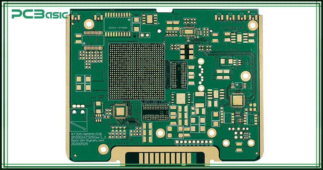
A PCB may function on paper. But to work in the real world—at scale, under heat, stress, and real-life manufacturing tolerances—it needs to be manufacturable.
That’s where DFM comes in. It’s not fancy. It doesn’t make your board prettier. But it does make it real. It saves cost. It prevents mistakes. And it keeps your timeline under control.
The best engineers design for the shop floor, not just the lab bench. If you want reliable builds and predictable yields—make DFM part of your design process.

Assembly Enquiry
Instant Quote
Phone contact

+86-755-27218592
In addition, we've prepared a Help Center. We recommend checking it before reaching out, as your question and its answer may already be clearly explained there.
Wechat Support

In addition, we've prepared a Help Center. We recommend checking it before reaching out, as your question and its answer may already be clearly explained there.
WhatsApp Support

In addition, we've prepared a Help Center. We recommend checking it before reaching out, as your question and its answer may already be clearly explained there.