Global high-mix volume high-speed PCBA manufacturer
9:00 -18:00, Mon. - Fri. (GMT+8)
9:00 -12:00, Sat. (GMT+8)
(Except Chinese public holidays)
Global high-mix volume high-speed PCBA manufacturer
9:00 -18:00, Mon. - Fri. (GMT+8)
9:00 -12:00, Sat. (GMT+8)
(Except Chinese public holidays)
HomePage > Blog > Knowledge Base > The Ultimate Guide to Designing 2-Layer PCBs
As electronic devices become smaller and more powerful, it is important to design circuit boards (PCBs) that are both efficient and cost-effective.
2-layer PCB, also known as double-sided PCB, has become one of the most popular circuit board types because of its simple structure and practical function. Whether it is an electronics enthusiast or a professional engineer, as long as you master the design skills of 2-layer PCBs, understand their standard thickness and basic design rules, you can make a circuit with good performance and high reliability.
This article will introduce the structure, production method and practical use of 2-layer PCBs in detail to help you better design and apply this circuit board.

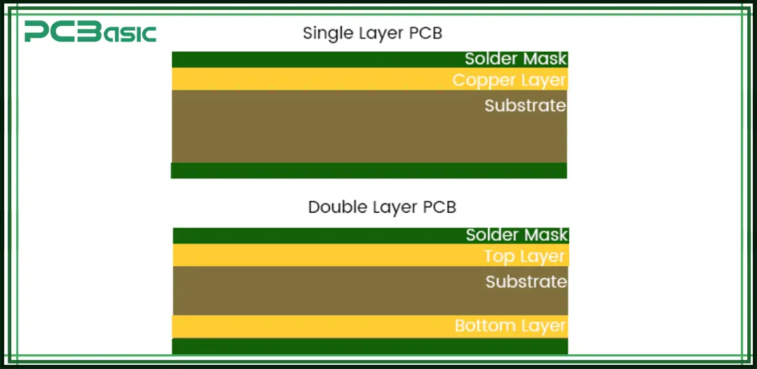
A 2-layer PCB has two layers of conductive copper, distributed on the top and bottom sides of the board. Unlike a single-layer PCB that can only have routing and install components on one side, a 2-layer PCB can route and install components on both sides, making the design more flexible.
Compared with the single-layer board, the 2-layer PCB can accommodate more circuits, more powerful, while the price is not too expensive, and it is often used in various electronic products such as televisions, home appliances, industrial equipment and medical instruments.

The 2-layer PCB thickness generally ranges from 0.6mm to 1.6mm, and common products will choose this range. The specific thickness depends on whether your product is large or small, where it is used, whether it needs good heat dissipation, and how much space is available inside the device.
Here is a brief description of some common thicknesses:
• 1.0mm: Suitable for lightweight and compact devices, such as handheld devices and portable electronics. It’s also light, strong enough.
• 1.6mm: The most common standard thickness. Most TVs, routers, and home appliances use this thickness. It offers moderate cost and stable quality.
• 0.8mm: Ideal for small, compact products, such as wearable devices, embedded modules, etc. It's thinner, more flexible and easier to fit into compact designs.
Choosing the right 2-layer PCB thickness is very important. It not only makes the circuit board stronger, not easy to bend, but also ensures the stability of signal transmission. Especially those electronic products with high-precision requirements, the effect is more obvious.
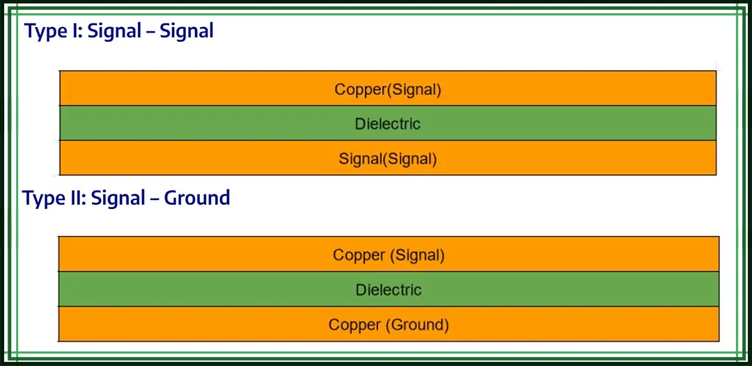
The standard stack-up structure of a 2-layer PCB typically consists of three parts:

Top Layer: Also known as the signal layer or component layer. This is where electronic components and routing are placed. Most circuit traces, pads, chips, resistors and other components are mounted on this side.
Dielectric Core Layer: This is the insulating material sandwiched between the top and bottom copper layers, commonly made of FR-4. Its purpose is to isolate the two copper layers to prevent short circuits while also providing structural support and stability to the 2-layer PCB.
Bottom Layer: It functions as either a signal layer or a ground/power layer. Like the top layer, it's a copper layer that allows circuit routing and connections, enhancing wiring flexibility and electrical performance.
This structure is both simple and practical, making the 2-layer PCB suitable for most common electronic devices such as consumer products, industrial control boards, and medical equipment. While meeting electrical performance requirements, it's also easy to manufacture and assemble. That's why 2-layer PCBs are widely used in consumer electronics, industrial controls, and medical devices.

When designing a 2-layer PCB, following strict 2-layer PCB design rules is key to ensuring reliability and manufacturability. These rules typically include:
Well-applied 2-layer PCB design rules ensure signal integrity and reduce manufacturing defects.
Because of the simple structure and advantages over single-layer PCBS, 2-layer PCBs are widely used in:
A single-layer PCB is a circuit board with only one side of the circuit. This side is usually covered with a layer of copper, used to connect electronic components. It does not have many internal lines like a multilayer PCB and can only route signals on one side.

Let’s compare the two in a table:
|
Feature |
Single-Sided PCB |
2-Layer PCB |
|
Copper Layers |
1 |
2 |
|
Component Density |
Low |
Moderate |
|
Routing Flexibility |
Limited |
Higher |
|
Cost |
Lower |
Slightly Higher |
|
Application Complexity |
Basic |
Intermediate |
PCBasic is a trusted PCB assembly manufacturer with a strong reputation for quality, speed, and innovation. Backed by over 10 years of experience in PCB design and project management, our team combines deep technical knowledge with efficient execution to deliver high-performance circuit board solutions across industries.
We maintain close collaborations with PhD research teams from leading universities, advancing industry-academia innovation in electronic manufacturing.

With multiple factory locations, we provide flexible production capacity:
• A Shenzhen factory for agile, small-batch and quick-turn prototyping
• A Huizhou facility optimized for high-volume production
PCBasic also operates its own precision CNC machining center and in-house stencil & fixture factory, enabling stencil delivery within 1 hour and rapid fixture customization.
Our intelligent electronic components central warehouse ensures real-time inventory control and traceability. We guarantee 100% original and genuine components, with a one-click BOM import and instant quoting system to simplify your procurement process.
Certified as a National High-Tech Enterprise, PCBasic holds multiple international certifications, including ISO 13485, IATF 16949, ISO 9001, ISO 14001, and UL. As an IPC member, we've earned over 20 national patents for quality inspection and production management systems—ensuring every board we build meets the highest standards of precision and reliability.
A 2-layer PCB is a cost-effective and efficient solution for many electronic designs. From understanding its basic structure and 2-layer PCB thickness to applying the right 2-layer PCB design rules, mastering the double-sided PCB can elevate your product’s performance and reliability.
Looking for a trusted 2-layer PCB manufacturer and assembler? Contact PCBasic to bring your ideas to life—fast, precise, and dependable.

Assembly Enquiry
Instant Quote
Phone contact

+86-755-27218592
In addition, we've prepared a Help Center. We recommend checking it before reaching out, as your question and its answer may already be clearly explained there.
Wechat Support

In addition, we've prepared a Help Center. We recommend checking it before reaching out, as your question and its answer may already be clearly explained there.
WhatsApp Support

In addition, we've prepared a Help Center. We recommend checking it before reaching out, as your question and its answer may already be clearly explained there.