Global high-mix volume high-speed PCBA manufacturer
9:00 -18:00, Mon. - Fri. (GMT+8)
9:00 -12:00, Sat. (GMT+8)
(Except Chinese public holidays)
Global high-mix volume high-speed PCBA manufacturer
9:00 -18:00, Mon. - Fri. (GMT+8)
9:00 -12:00, Sat. (GMT+8)
(Except Chinese public holidays)
HomePage > Blog > Knowledge Base > N Type and P Type Semiconductors - Explained
P-type and N-type semiconductors, are the most common semiconductors (e.g., diodes, transistors, and integrated circuits). These two semiconductor types work together in electronic devices to create the various electronic components we use every day.
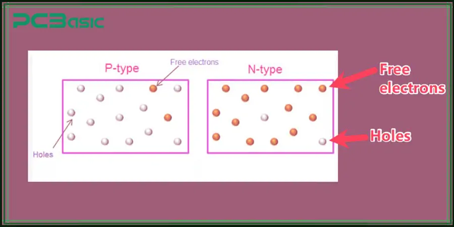
Today, this article will delve into the basic concepts of P-type and N-type semiconductors, and their key applications in modern electronic devices. It will also compare the differences between P-type and N-type semiconductors. Hopefully, after reading this article, it will help you better understand how these two semiconductors work together and provide power for the realization of various high-performance electronic components.
Before understanding the P Type and N type semiconductors, let's first understand what is a semiconductor.
As has already been said, semiconductors are not a single material, but are made by doping different elements. That's right, the essence of a semiconductor is a material with appropriate electrical conductivity between a conductor and an insulator, by doping different elements (such as trivalent and pentavalent elements) to form P-type and N-type semiconductors. This means that semiconductors can conduct electricity under some conditions and not under others.
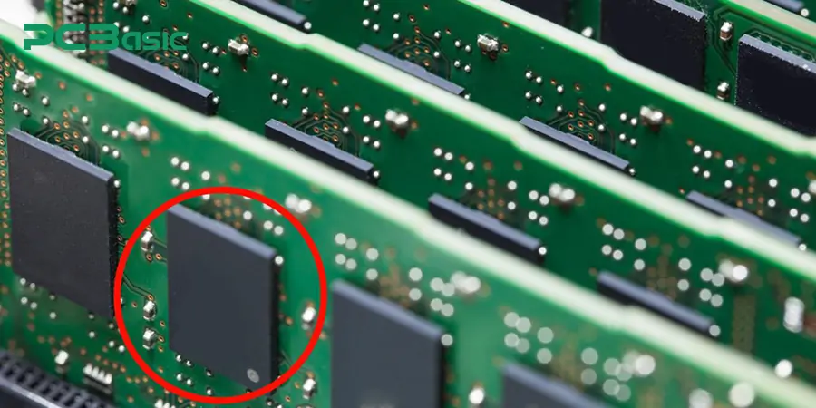
The application of semiconductors is very wide, used in a variety of devices, such as computer processors, memory chips, solar cells, leds and transistors. It can be said that semiconductors are the basis for almost all electronic circuits to achieve functions such as amplification, switching and signal modulation.
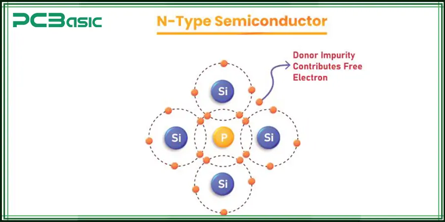
N-type semiconductor is a semiconductor material made by incorporating a pentavalent element *, such as phosphorus, arsenic, or antimony. The incorporation of these pentavalent elements greatly increases the number of electrons in N-type semiconductors compared to intrinsic semiconductors *.
The main charge carriers of N-type semiconductors are free electrons, which come from the incorporated pentavalent elements that can move freely in the crystal. When an external electric field is applied to the semiconductor, these free electrons migrate under the action of the electric field, forming an electric current. In N-type semiconductors, due to the higher concentration of electrons and the smaller number of holes (that is, where electrons are missing in the crystal), they conduct electricity much less than free electrons. The "N" of an N-type semiconductor means that its main carrier is a negatively charged electron; In electronic devices, it is mainly used as a conductive medium for current.
*Pentavalent elements have five outer electrons, four of which form covalent bonds with other atoms in the silicon lattice, while the remaining one does not participate in covalent bond formation, forming free electrons, which give N-type semiconductors higher electrical conductivity.
*Intrinsic Semiconductor refers to pure semiconductor materials that are not doped with any other elements. Its conductivity is determined only by the properties of the material itself, rather than being adjusted by external impurities such as doped elements.
Typically, N-type semiconductors are made using silicon (Si) as a substrate by incorporating doping materials such as pentavalent elements (such as phosphorus, arsenic, or antimony). These doping pentavalent elements will have an extra electron, forming four covalent bonds with the silicon atom, leaving one free electron that does not participate in the bond. This free electron, which does not belong to any atom, is free to move through the crystal structure, thus improving the material's ability to conduct electricity.
The doping process is a key step in changing the properties of a semiconductor. By adjusting the concentration of incorporation, the conductivity of N-type semiconductors can be precisely controlled.
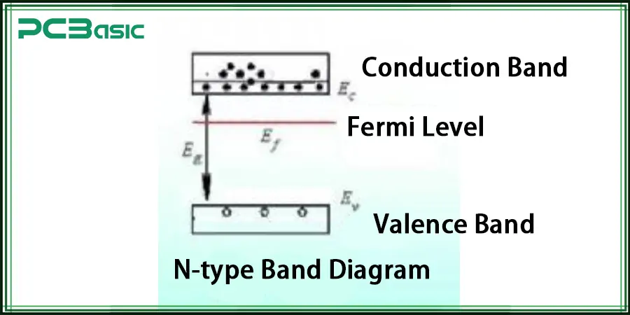
N-type band diagrams are diagrams that describe the energy distribution of electrons inside N-type semiconductors, helping us understand how electrons in semiconductor materials are distributed in different energy bands, and how they are affected by factors such as doping (such as incorporation of pentavalent elements) and external electric fields.
Conduction Band: A band in which electrons can move freely. (This is where electrons are able to move freely through the material, allowing them to conduct electricity.)
Valence Band: The highest energy band that an electron can occupy without external excitation. (Electrons in valence bands usually do not flow freely.)
Bandgap: The area of energy between the conduction and valence bands.
Fermi Level: A reference energy level indicating the energy state of an electron.
Free Electrons: The added pentavalent element provides additional electrons, which fill the vacancy near the conduction band, thus forming free electrons.
For N-type semiconductors, the Fermi level is closer to the conduction band region with respect to the conduction band. Conduction bands are high energy bands in which electrons can move freely through the semiconductor. Because there are a large number of free electrons in N-type semiconductors, these electrons can enter the conduction band under the action of an external electric field, thus achieving conduction. In the band diagram, the bandgap between the conduction band and the valence band is usually large, and the electrons need to overcome certain energy barriers to jump from the valence band to the conduction band. However, in N-type semiconductors, because the added pentavalent elements provide additional electrons, these electrons do not need to cross the band gap, but are directly near the conduction band, allowing electrons to flow freely.
Thanks to the presence of free electrons, N-type semiconductors have high conductivity and can conduct electricity under the action of external electric fields. When an electric field is applied to an N-type semiconductor, free electrons flow from a region of high potential to a region of low potential, generating an electric current. The transport efficiency of free electrons is very high, and the conductivity of N-type semiconductors is usually strong.
The conductivity of N-type semiconductors is affected by temperature and doping concentration. The higher the temperature, the greater the number of free electrons in the material, and the stronger the conductivity. The higher the doping concentration, the greater the number of free electrons in the semiconductor, and the electrical conductivity will increase accordingly.
N-type semiconductors are widely used in various electronic devices. For example, diodes, transistors, solar cells, voltage regulators and integrated circuits.
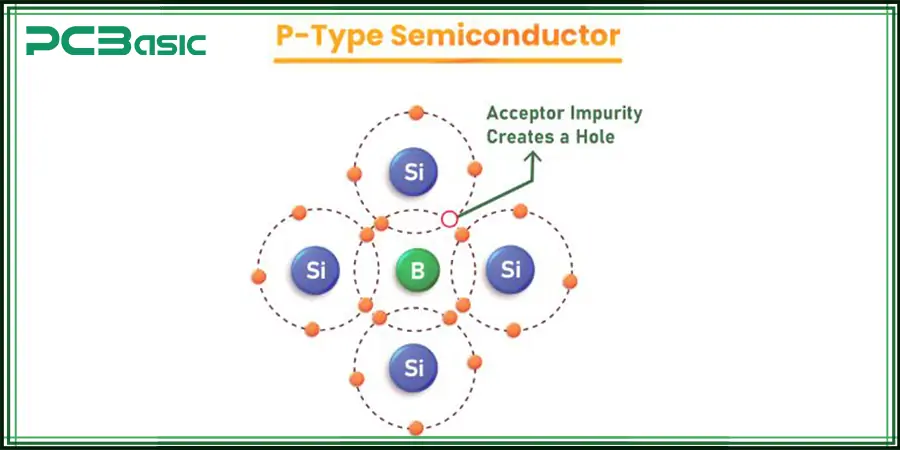
P-type semiconductors are formed by doping trivalent elements (such as boron, aluminum, gallium, etc.) into pure silicon (Si) or germanium (Ge). After the doping of these trivalent elements, a large number of holes (positive charge carriers) are formed in P-type semiconductors, which significantly increases their electrical conductivity. Unlike the free electrons of N-type semiconductors, the main charge carriers of P-type semiconductors are holes, which can move freely in the semiconductor crystal to allow the current to pass through.
P-type semiconductors usually use silicon (Si) as a substrate with trivalent elements (such as boron, gallium, aluminum, etc.). These trivalent elements have three outer electrons, and when they combine with silicon atoms, each trivalent element forms a covalent bond with four silicon atoms, but because the trivalent element lacks an electron, this creates a hole. The holes can be viewed as positively charged charge carriers that can move through the crystal and thus conduct current.
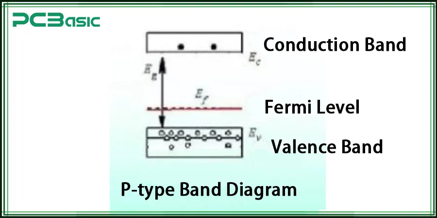
In the same way that N-type band maps have been described previously, P-type band maps help us understand how electrons are distributed in semiconductor materials and how they are affected by factors such as doping (such as incorporation of trivalent elements) and external electric fields. The key elements of a P-type semiconductor band map are the same as those of an N-type semiconductor, but the band map is different, as shown below.
There are a large number of holes in P-type semiconductors, and the flow of holes enables P-type semiconductors to conduct electricity. Under the action of an applied electric field, the hole moves from the region of high potential to the region of low potential, resulting in an electric current.
The higher the temperature, the greater the number of holes in the P-type semiconductor and the stronger the conductivity. The higher the doping concentration, the greater the number of holes in the P-type semiconductor, the stronger the conductivity.
P-type semiconductors are also widely used in various electronic devices, such as diodes, transistors, photodiodes, etc.
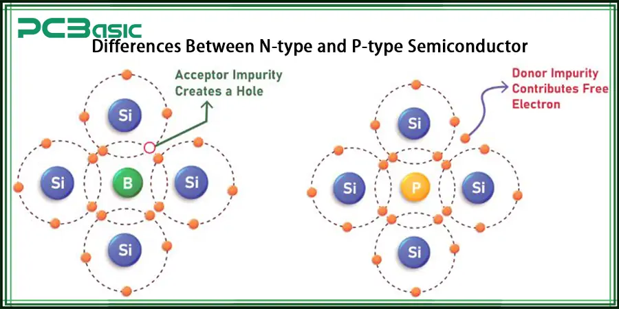
The definition, doping process, band diagram, electrical conductivity and applications of N-type and P-type semiconductors have been described. Now let's take a look at the differences between the two types, as shown in the table.
|
Item |
P-type Semiconductor |
N-type Semiconductor |
|
Doping Element |
trivalent elements (e.g., boron) |
pentavalent elements (e.g., phosphorus) |
|
Main Carrier |
holes (positive charge) |
free electrons (negative charge) |
|
Carrier Movement |
Holes move under the influence of the electric field |
Free electrons move under the influence of the electric field |
|
Fermi level |
Close to the valence band |
Close to the conduction band |
|
Conduction Mechanism |
Conducts through the movement of holes |
Conducts through the movement of free electrons |
|
Application Difference |
Used in PNP transistors, photodiodes, etc. |
Used in NPN transistors, MOSFETs, etc. |
|
Application |
PN junction diodes, PNP transistors |
NPN transistors, N-type MOSFETs |
|
Role in Circuits |
Primarily used to construct the positive terminal |
Primarily used to construct the negative terminal |
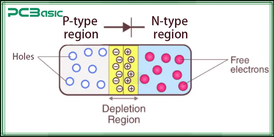
PN junction means the combination of P-type and N-type semiconductors. The combination of P-type and N-type semiconductors forms many fundamental electronic devices. Now, let’s learn about it.
In the process of PN junction formation, several phenomena will occur: carrier diffusion, formation of depletion zone, and internal electric field.
Carrier diffusion refers to the diffusion of free electrons in N-type semiconductor to P-type semiconductor and the diffusion of holes in P-type semiconductor to N-type semiconductor during the formation of PN junction. The reason for this is that the high concentration of carriers will naturally spread to the low concentration region until the carrier concentrations on both sides tend to balance. Then, as electrons diffuse from the N-type semiconductor to the P-type semiconductor, filling the holes in the P-type semiconductor, negative ions form. On one side of the N-type semiconductor, the flow of electrons leads to a lack of free electrons, forming positive ions. At this point, the binding region of holes and electrons forms a depletion region, with no charge carriers and no current flowing through it. In the depletion region, the electric field formed in the PN junction region due to the charge separation between positive and negative ions is called the internal electric field or the intrinsic electric field.
The conduction characteristic of PN junction refers to the current conduction or blocking behavior of PN junction under different voltage conditions. PN junction is mainly affected by the following two conditions:
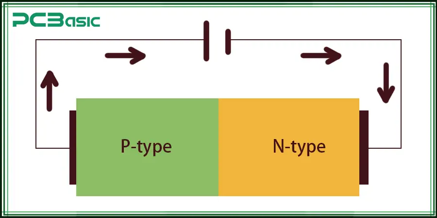
Forward bias: that is, when the P-type semiconductor is connected to the positive terminal of the power supply and the N-type semiconductor is connected to the negative terminal of the power supply, the externally applied voltage will reduce the influence of the internal electric field, so that the holes in the P-type semiconductor and the electrons in the N-type semiconductor can pass through the PN junction to form a current. At this time, the PN junction can conduct electricity.
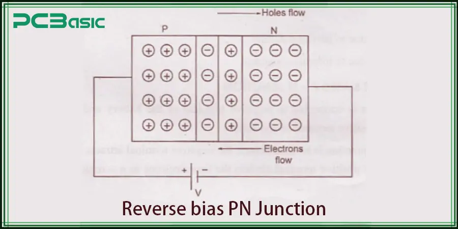
Reverse bias: When the P-type semiconductor is connected to the negative electrode of the power supply and the N-type semiconductor is connected to the positive electrode of the power supply, the externally applied voltage will increase the strength of the internal electric field, making it difficult for electrons and holes to pass through the PN junction. At this time, the PN junction does not conduct electricity. Of course, when the applied voltage is large enough to break down the PN junction, the current will suddenly increase. These are the conductive properties of the PN junction, which make the PN junction very important in electronic devices. Diodes, for example, use these conductive characteristics of the PN junction to control the flow and size of the current.
In the PN junction, the P-type semiconductor provides holes as the main charge carriers and moves towards the N-type semiconductor under the action of an electric field. N-type semiconductors provide free electrons as the main carriers, which move towards P-type semiconductors under the action of an electric field. P-type semiconductor and N-type semiconductor cooperate with each other through diffusion and electric field action to form depletion zone and internal electric field, so that PN junction can effectively control the flow of current.
In a word, P-type and N-type semiconductors are the building blocks of modern electronics. Whether you're using them in diodes or transistors, understanding their properties and differences is critical to designing and optimizing electronic circuits. I hope this article has been helpful to your understanding of P-type and N-type semiconductors.

Assembly Enquiry
Instant Quote
Phone contact

+86-755-27218592
In addition, we've prepared a Help Center. We recommend checking it before reaching out, as your question and its answer may already be clearly explained there.
Wechat Support

In addition, we've prepared a Help Center. We recommend checking it before reaching out, as your question and its answer may already be clearly explained there.
WhatsApp Support

In addition, we've prepared a Help Center. We recommend checking it before reaching out, as your question and its answer may already be clearly explained there.