Global high-mix volume high-speed PCBA manufacturer
9:00 -18:00, Mon. - Fri. (GMT+8)
9:00 -12:00, Sat. (GMT+8)
(Except Chinese public holidays)
Global high-mix volume high-speed PCBA manufacturer
9:00 -18:00, Mon. - Fri. (GMT+8)
9:00 -12:00, Sat. (GMT+8)
(Except Chinese public holidays)
HomePage > Blog > Knowledge Base > What are Circuit Board Traces?
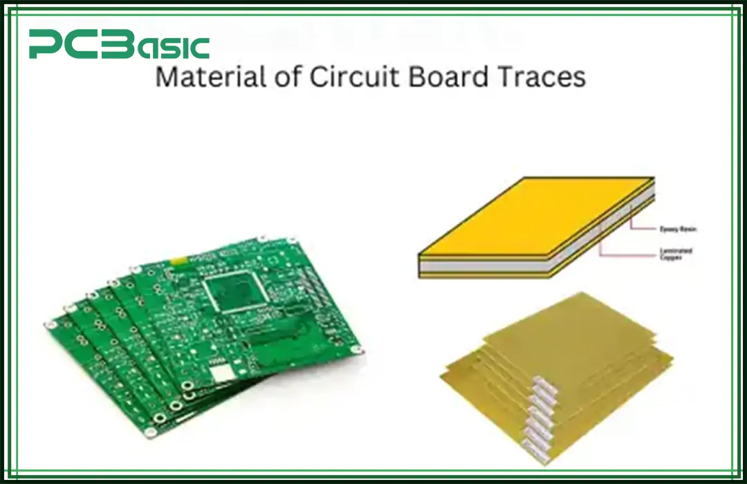
The circuit board traces are etched directly on the substrate of the PCB boards. They are also known as pathways. These traces are similar to wires. The basic purpose of these traces is to transfer signals or power to PCB components. For instance, relays, resistors, terminals, capacitor cases, and conductors. So how do PCB engineers handle this situation? They make PCB traces from copper foil in a narrow width.
So the interesting point is that these traces have transformed the electronic fields. For example, these traces completely eliminate traditional wiring methods. The manufacturers use them for reliability and as standardized pathways nowadays.
In very simple words, circuit board traces are the thin metal lines you generally see on a circuit board. Just take them like tiny roads that electricity travels on. So, when you power up a device, electricity flows along these traces. The purpose is to connect all the parts together.
You see, these traces are significantly important because without them, your electronics wouldn't work at all! The main point is they replace messy wires, making devices smaller and more reliable. Why is it important? Because nearly every gadget you use has them inside.

Check out these common materials of PCB trace:
● Copper (Cu)
● Aluminum (Al)
● Silver (Ag)
● Gold (Au)
● Nickel (Ni)
PCB manufacturers incorporate copper (Cu) as a common manufacturing material. Consequently, in PCBs, it is leveraged to construct thin pathways for transmitting signals. Do you know it offers tremendous characteristics? That makes it an indispensable choice. For example, electrical conductivity, economical prices, and compatibility.
The unique features of copper and its performance help the engineers. It enables them to produce productive electric gadgets. Somewhat it is the most used material due to its durability, reliability, and resistance to handling damaging characteristics.
Properties:
● High Electrical Conductivity
● Thermal Conductivity
● Ductility
● Economical
● Resist rust
● Strength-to-weight ratio
● Reliability
Applications:
Microstrip Transmission Lines
The copper traces are used to improve the high-frequency signals in microstrip transmission lines. You can customize the traces of copper with custom widths and thicknesses.
Power Amplifiers
The manufacturers employ copper traces in power amplifiers so that they can distribute the power and regulate the output level.
High-Frequency Circuits
Copper traces improve the performance of high-frequency circuits. That includes radar or communication systems. They provide good electrical conductivity and low control resistance.
Radio Frequency Identification (RFID)
The manufacturer attaches copper traces to the radio frequency identification. That transmits data wirelessly. It is also used for storage purposes.
MEMS Devices
These traces are used in microelectromechanical devices. It combines the mechanical and electronic elements on a single trip.
Solar Panels
Solar panels are outdoor applications. They required extensive properties of materials that can resist corrosion and critical environmental aspects. That is why the engineer inserts the copper traces in the PCBs of solar panels.
Signal Integrity
Copper traces are widely used in electronic devices. That improves the signal integrity. It reduces the electromagnetic interference (EMI) and crosstalk.
As we all know, aluminum has been used in manufacturing techniques for decades. It is easily available on the market. This metal has excellent corrosion resistance attributes. Aluminum PCB traces are built through a manufacturing process called a metal core.
Using aluminum alloys to construct circuit board traces is pivotal for lightweight products. Its thermal conductivity characteristics help dissipate heat generation during transmission operations.
Properties:
● Lower Electrical Conductivity
● Excellent Thermal Conductivity
● Lightweight
● Protection from corrosion
● Durable
● Reliable
Applications:
Cryogenic Electronics
Aluminum traces function as superconducting wiring. That enables the signal supply. This is why it maintains a high-power flow at cryogenic temperatures. That significantly needs low temperatures. The cryogenic electronics products are quantum computing or progressive research tools and scientific instruments.
Transparent PCBs for X-ray systems
Aluminum traces contain atomic numbers. They are used for their lower X-ray attenuation in X-ray systems. It expertly reduces the absorption of radiation than copper. These traces become transparent when the consumer performs an x-ray of an object. It enables the clear observation results.
Nuclear beam applications
As we have discussed, the aluminum alloys provide good thermal conductivity. Therefore, the manufacturer uses them to make nuclear beam applications. That contains high radiation levels. The aluminum traces manage heat dissipation. Detection approaches, nuclear instrumentation, and particle accelerator electronics use these traces. That helps them reduce heat generation.
LED Lighting Systems
LED lighting continues to produce heat during operations. It needs the elements that transfer this excessive heat away. Aluminum traces are the best option to control overheating.
Aerospace and Automotive
The consumers harness aluminum traces in various industrial systems. These traces eliminate the overheating during operations. In aerospace and automotive industries, aluminum traces are used in vehicles, aircraft, household products, and consumer devices. These devices incorporate aluminum traces as a heat sink.

Silver is cheaper than gold. It supplies high conductivity to heat and corrosion resistance features. That can enable the improved soldering. The manufacturers harness this material to increase the surface finish of copper. In accordance, it produces a protective layer on the traces of board assemblies.
Properties:
● Effectively dissipates heat.
● Highest Electrical Conductivity.
● Resists oxidation better than copper.
● Expensive
Applications:
Circuit Boards with High-Frequency
The silver traces carry good current capacity. That supports the signal transmission. These traces eliminate the interruption in signals at high frequencies. They are used in RF circuits and products with precise signal transmission.
Medical Apparatuses
Silver traces are used in pacemakers and diagnostic devices. What is the basic purpose? These traces are inserted into PCBs to improve equipment performance. It allows them to collect accurate information from sensitive machines.
Military Systems
Silver metal is an economical choice substitute for copper. Therefore, it is widely used in military systems. It protects marine applications from extreme conditions.
Consumer Electronics
PCB companies like PCBasic focus on making safe and reliable electronics. Silver traces provide an additional layer for soldering to the PCB. This increases the application's lifespan and wearability.
Gold is an expensive material compared to other metals. However, gold has a range of properties. You can incorporate this material to create durable traces of circuit boards. Besides its primary features ( corrosion resistance, flexibility, and thermal capacity), it enables strong bonding among wires. This material is biocompatible and melts quickly. The manufacturer can recycle this component for novel yield production.
Properties:
● Excellent resistance to oxidation and corrosion
● Biocompatible
● Surface finish
● Costly
● Flexibility
● Easy to melt
● Good soldering
● Lead-free
Applications:
Edge connectors and switch contacts
The gold substance is used in PCB to coat the edge connectors and switch contacts. That helps in making a stable connection over time.
Microelectronics
The contribution of microelectronics like ICs or semiconductors is high in PCBs. That is why gold is chosen to stabilize its conductive features.
Electronic Equipment
Gold-plated columns are used in electronic gadgets such as computers, wearable items, and smartphones. They are connected to the motherboard via secondary circuits.
Spacecraft and satellites
The spacecraft and satellite applications use gold traces in PCB to withstand risky climates. These traces control their communication transmission and power systems effectively.
Nickel material is commonly used to create double-coat layers on copper plates in PCB. The first layers protect the plates from rust and oxidation. Similarly, the second layer extends its longevity. This metal also acts as the barrier between the solder's parts and copper.
Properties:
● Offer strong resistance to oxidation.
● Enhance the lifespan
● Solderability
● Moderate electrical conductivity
● Hardness
Applications:
ENIG Plating
The electroless nickel immersion gold plating is constructed on PCB. That furnishes an additional layer of protection from oxidation.
Plated Through-Holes
The engineer uses nickel to plate through holes. They improve the mechanical strength of multi-layer PCBs.
Connectors and contact points
PCBs' connectors and contact points need strong integration for long-term use. Therefore, nickel material is used for soldering and offering harnesses to the components.

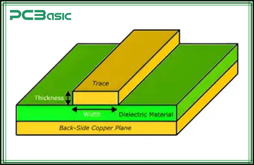
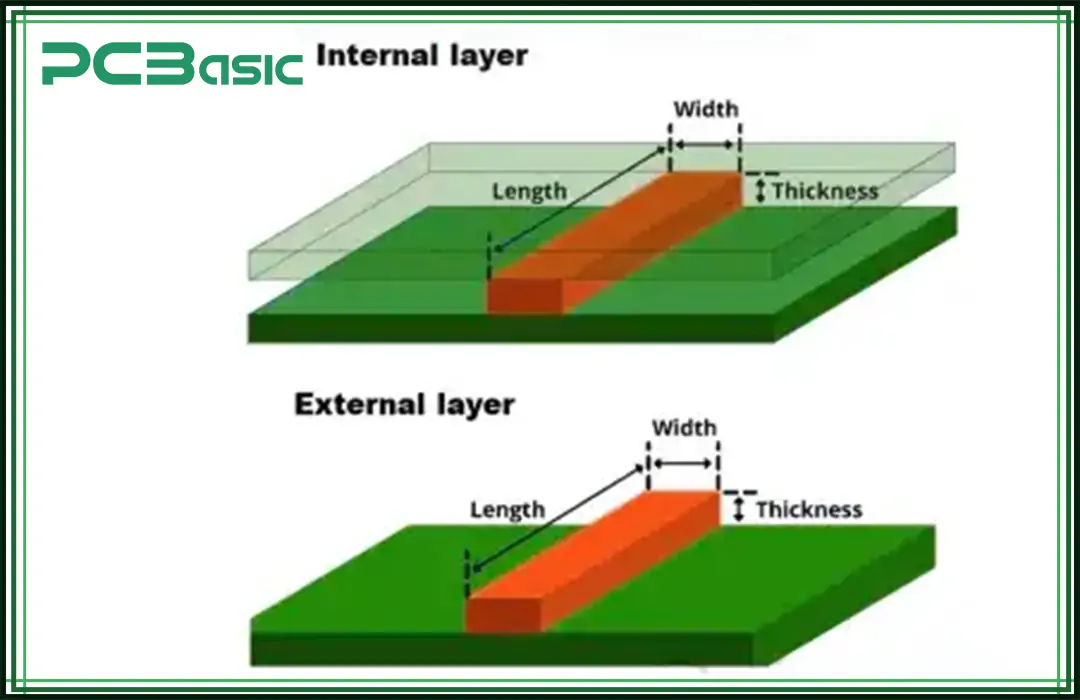
PCB trace thickness is known as the width and height of the trace. It can be decided depending on the project designs. Usually, the thickness of a circuit board trace ranges from 0.008 inches to 0.240 inches. Consider the following factors when determining the thickness of the PCB trace:
● Standard thickness
● Trace width
● Trace termination
● Trace size calculator
The standard thickness of PCB traces for simple to industrial applications is around 0.5 oz/ft2 to 2 oz/ft2. However, heavy-duty projects with high-voltage power need 6 oz/ft2 or more.
The determination of trace width is commonly fixed and specified by the constructor of the PCB. It refers to the thin line of conducting copper. That carries the signal transmissions.
One more thing a reader should remember is that the junction of traces and pads also influences trace thickness. The trace width is mainly decided according to the pads' width in the SOIC footprints.
The manufacturers of PCB also harness trace size calculators to weigh trace thickness. It helps them to choose the appropriate dimensions to avoid overheating and shock risk.

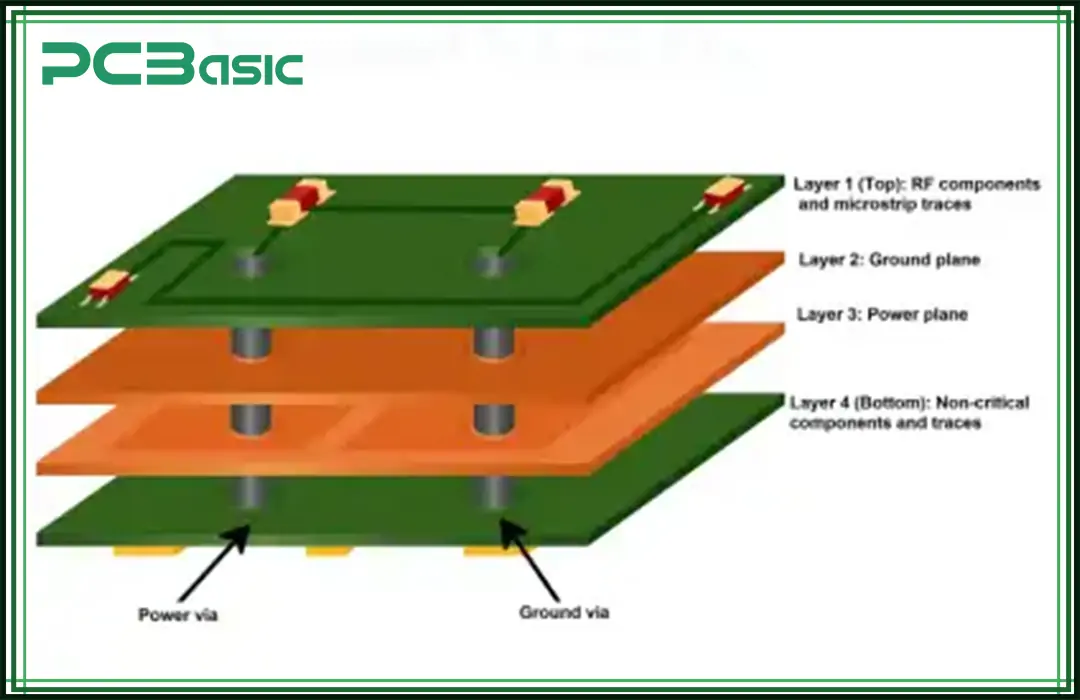
What is PCB trace width vs current? If we make it very simple, you can say that the relationship between the PCB trace and the current indicates the transmission capacity. The size of the trace thickness drastically influences the voltage of low to high current power. Therefore, the right size selection is essential to increasing the reliability of the PCB.
● IPC-2221 Standard
● Factors to Consider
IPC-2221 is the most effective approach. That helps the manufacturers determine the accurate size of trace thickness. It indicates several crucial aspects in the form of formulas and charts of current capacity and temperature rise. Look at the chart mentioned below. This will guide you on how to choose the thickness size. It is based on the current capacity for external and internal layers.
|
Current (Amps) |
External Trace Width (mil) |
Internal Trace Width (mil) |
External Trace Width (mil) |
Internal Trace Width (mil) |
|
|
(10°C rise) |
(10°C rise) |
(20°C rise) |
(20°C rise) |
|
0.5 |
6 |
12 |
4 |
7 |
|
1 |
12 |
24 |
7 |
14 |
|
2 |
20 |
40 |
12 |
24 |
|
3 |
30 |
60 |
20 |
40 |
|
5 |
50 |
100 |
30 |
60 |
|
10 |
100 |
200 |
60 |
120 |
|
15 |
150 |
300 |
100 |
200 |
● Current Flow
● Permissible Temperature Rise
● PCB Layer
So, when a trace breaks on a circuit board, you can repair it yourself. The basic point is you need to create a new path for electricity to flow. First, clean the damaged area to PCB repair. You see, any dirt will prevent the repair from sticking. Then use conductive paint, solder, or a thin wire to reconnect the broken trace.
It is the main point to make sure the new connection is secure and making full contact. Why is it important? Because a weak repair will fail again soon. Understand? If you have fine circuit board trace repair, they will save you from replacing the entire board!
Circuit board traces are the standard pathways of circuit boards. They distribute the transmission of signals across all elements. The manufacturer can choose from several materials to construct their desired traces. These traces are widely used in a plethora of applications for signal integrity. The thickness and width of traces directly impact their performance. Therefore, consider the specific aspect while designing your PCB traces with functional qualities.

Assembly Enquiry
Instant Quote
Phone contact

+86-755-27218592
In addition, we've prepared a Help Center. We recommend checking it before reaching out, as your question and its answer may already be clearly explained there.
Wechat Support

In addition, we've prepared a Help Center. We recommend checking it before reaching out, as your question and its answer may already be clearly explained there.
WhatsApp Support

In addition, we've prepared a Help Center. We recommend checking it before reaching out, as your question and its answer may already be clearly explained there.