Global high-mix volume high-speed PCBA manufacturer
9:00 -18:00, Mon. - Fri. (GMT+8)
9:00 -12:00, Sat. (GMT+8)
(Except Chinese public holidays)
Global high-mix volume high-speed PCBA manufacturer
9:00 -18:00, Mon. - Fri. (GMT+8)
9:00 -12:00, Sat. (GMT+8)
(Except Chinese public holidays)
HomePage > Blog > Knowledge Base > What is a Bare PCB?
One of the key components of electronic equipment, printed circuit boards (PCBs), control the function and operation of products, is indispensable. But the circuit board —which, by the way, is not simply a board. A board will go through various stage from design to product assembly and thus is referred to by a variety of names. In this blog, we will discuss bare PCB, and how it differs from an assembled board.
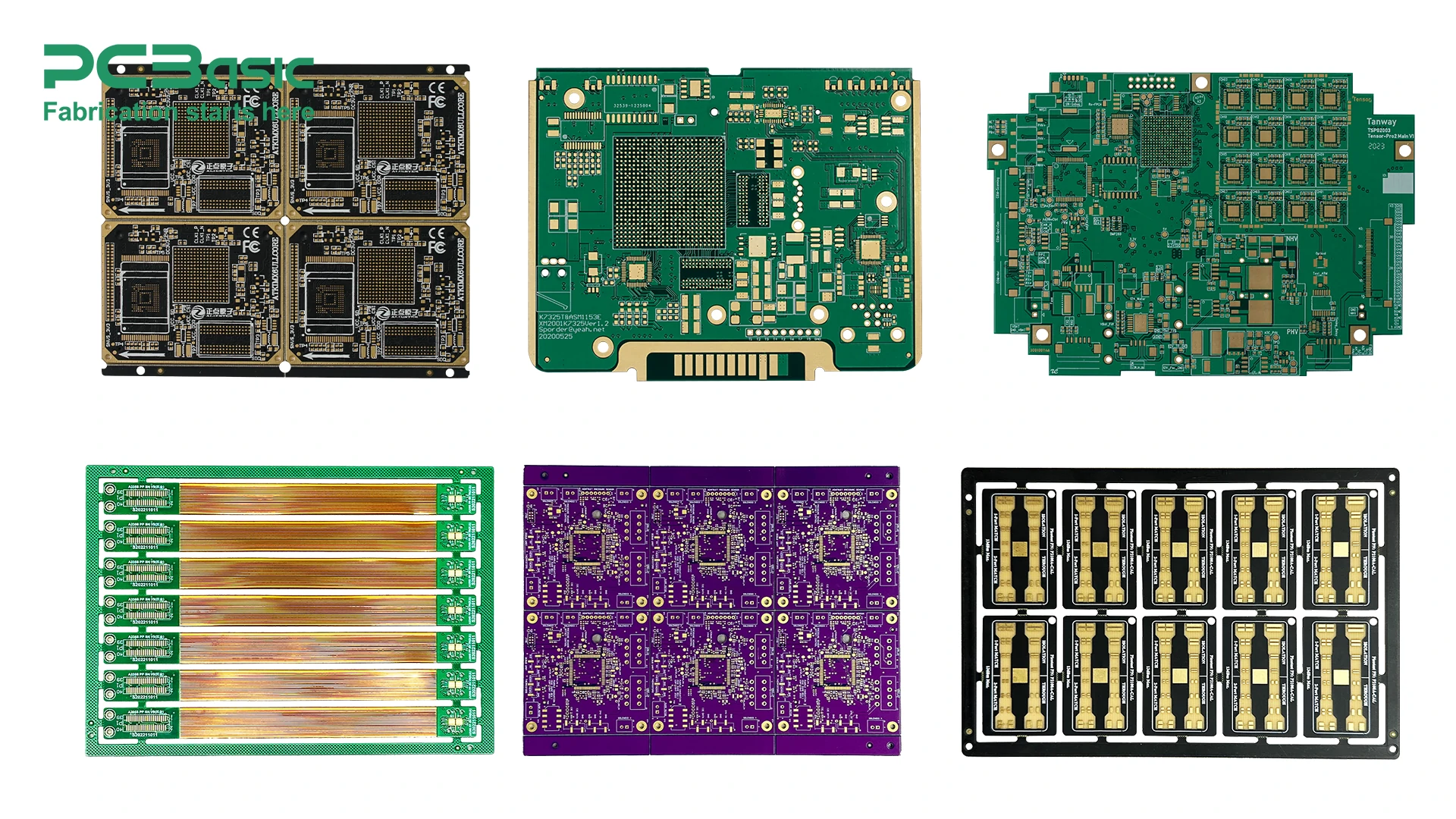
A bare PCB, also known as a bare board or bare printed circuit board, is a basic circuit board that is in the early stage of PCB manufacturing and has not assembled any electronic components, including only copper traces, pads, holes, and other basic circuit structures. As the core structure for building and supporting circuits in electronic devices, the bare PCB provides the function of mechanical support and electrical connection. And as the first step in assembling electronic devices, bare boards are critical to the performance of the entire product.
Layers: The bare PCB has a single-layer, double-layer and multi-layer structure according to the needs of the later stage.
Conductive Paths and Pads: The conductive paths and pads are distributed on the bare PCB. The conductive path is generally composed of copper foil and is a channel for electrical signal transmission. The pad is used to fix and connect electronic components in the later stage of the circuit board and is a key electrical interface in the assembly process. The design of the conductive path and pad needs to be very precise to achieve their specific circuit functions.
Materials: Bare circuit board substrates are typically made of glass fiber-reinforced epoxy resin (FR4) or other materials that provide insulation and structural strength.
Surface Finish: In order to protect the bare copper conductive layer from oxidation and improve solderability, bare circuit boards are generally subjected to surface finish such as HASL (Hot Air Solder Leveling) and ENIG (Electroless Nickel Immersion Gold).
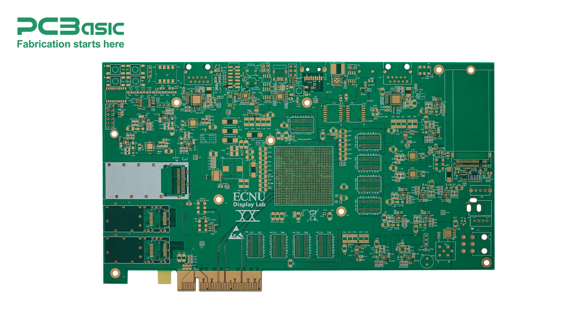
Bare circuit boards play an important role in the field of electronic design and manufacturing. As mentioned above, the bare circuit board is the core structure of the electronic device to build and support the circuit, providing the function of mechanical support and electrical connection for the device. But in fact, due to its unique features, its use is not limited to carrying components, but also covers design flexibility, production efficiency and quality control.
A bare board with only pads and conductive copper traces, designers can freely add electronic components according to circuit requirements, such as resistors, capacitors, transistors and integrated circuits, to achieve a variety of functions from simple circuits to complex systems.
At the same time, bare PCB is versatile, there is no need to redesign the board for each order, and bare PCB manufacturers can meet the needs of different customers through unified production. This significantly shortens design and manufacturing times and reduces development costs.
During the bare PCB design, designers invest a lot of effort to ensure that the design and production are accurate and ready for the subsequent assembly and manufacturing process to be highly automated. For example, through automatic pick-and place machine and wave soldering equipment, components can be quickly assembled on PCBs, enabling large-scale production and significantly improving production efficiency.
The bare circuit board is not only the basis of the product, but also has an irreplaceable role in the production process. In the initial stage of circuit board production, engineers will test the conductive copper trace and pad integrity of the bare PCB to ensure that the design is correct and meets the specifications, ensuring that each PCB meets the high standard of performance and reliability and providing a solid foundation for subsequent component assembly and product functionality.
In addition to the above applications, because of the simple components, the bare PCB is often used in teaching and experiments to help students and engineers familiarize themselves with the circuit design and manufacturing process.
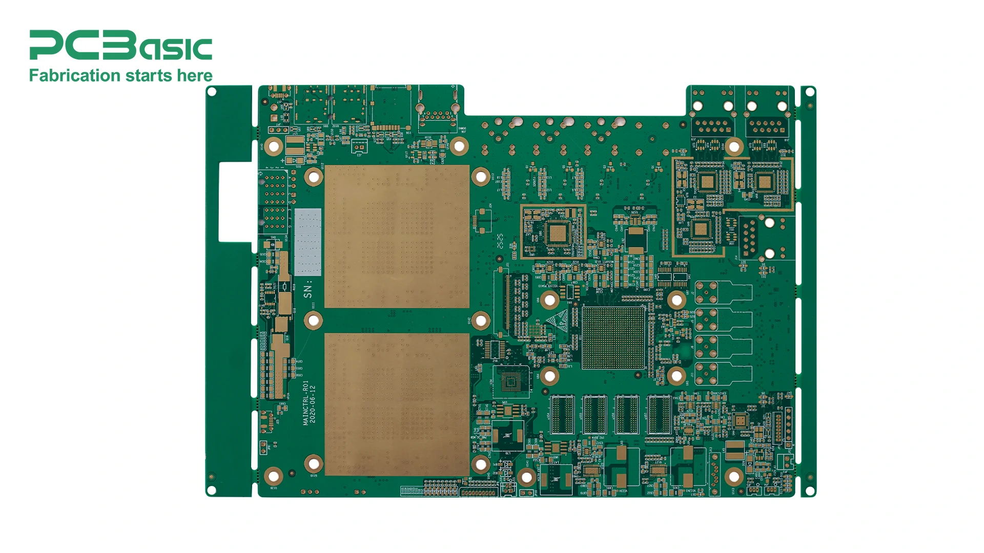
Bare Board Testing, or BBT, tests a bare PCB to ensure that the design, including its electrical connection, function, and integrity of the board meet requirements, avoiding design problems that may occur during or after assembly and saves costs and production time.
The bare board testing usually adopts the flying probe test, fixture-based test, automatic optical inspection (AOI) and X-ray inspection to carry out the following tests of bare boards:
The primary task of bare board testing is to detect whether there are electrical problems on the board, such as open circuits, short circuits and poor solder joints, to ensure that the bare PCB meets the requirements of the design and later requirements, so as not to affect the later component assembly and product function.
In PCB design, all electrical connections, including through holes, conductive traces and signal lines, must be laid out in accordance with specific electrical drawings and design rules, and ensure that the connection between different layers in the multi-layer circuit board is proper. Bare board testing ensures that these design requirements have been implemented correctly, and any errors or missed connections will be found during testing.
As mentioned above, conducting bare board testing can detect electrical design defects early and avoid massive rework or scrap caused by problematic boards entering the assembly process, saving time and material costs.
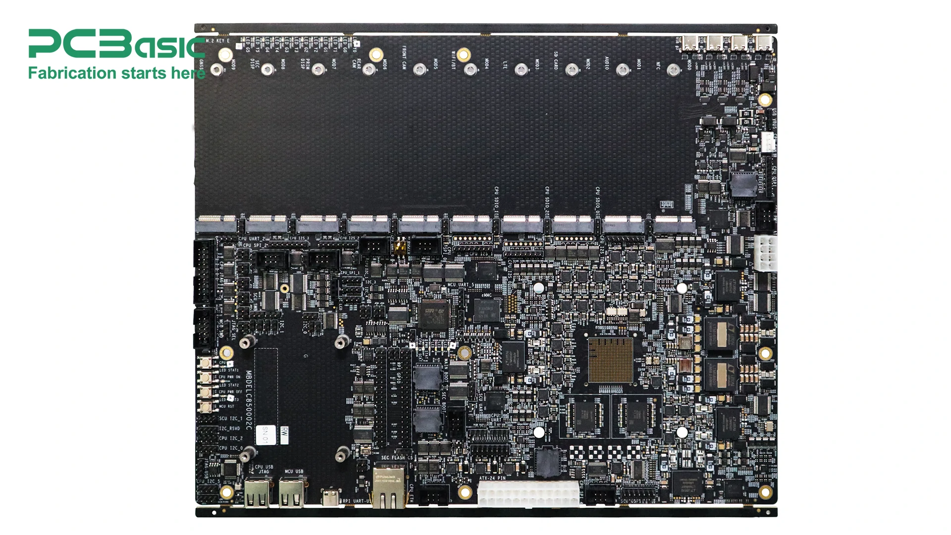
The manufacturing of a bare circuit board is the whole process of making a bare printed circuit board that does not have any electronic components like chips, resistors, and capacitors soldered to it. The bare PCB is the most basic form of a PCB, this stage comes before component assembly. You have design, material selection, board fabrication, and testing — multiple stages in this process.
Design Input: Design the circuit board layout based on EDA software, like Altium Designer, Eagle, or CAD. This is a physical representation of the design file.
Gerber File Generation: Once the design is finished, it gets transformed into Gerber Files, which are standard file strings for PCB manufacturing. These files contain the data used to make the circuit patterns.
Material Selection: The basic material of a bare PCB is generally copper-clad laminate, the latter generally is FR4 (epoxy fiberglass) or CEM-1 for substrate.
Substrate Cutting: The base material is trimmed to the desired dimensions, typically large panels being sliced into smaller boards.
The PCB substrate is thoroughly cleaned to remove surface contaminants, oils, and other impurities. This step ensures the success of the subsequent processes, such as etching, and is typically done using degreasing agents or water-based cleaning methods.
Photoresist Coating: Apply a layer of photoresist on copper surface. This photoresist will be light-sensitive, it means during the light exposure it only reacts in some photoresist the circuit patterns will be designed.
Exposure: The board is exposed to UV light with a photomask. The photoresist regions that are not exposed become hardened, while the photoresist regions that are exposed soften and can be taken away.
Developing: The PCB is then put into a developing solution, where any areas of the photoresist not exposed to light are washed away, leaving behind the intended circuit traces.
Copper Etching: The board goes through an etching process based on the photomask so that only the areas with no protected copper (uncovered by the photoresist) are removed, and only the desired circuit pattern is left. Solutions of ferric chloride, or copper chloride, are widely used for etching.
Pattern Inspection: The printed circuit board is inspected to make sure that the circuit pattern is correct and does not contain any shorts or opens.
Holes are drilled into the PCB as per design specifications using a CNC drilling machine or laser drilling. Those holes are called pads and they will be used for component leads or vias (connections between various layers of the PCB).
Electroless Copper Plating: Electroless copper plating is deposited onto through-holes and blind holes to create conductive paths in holes.
Electroplating: The PCB surface is occasionally electroplated with metals such as gold, silver, or tin that help to enhance the conductance, oxidation resistance, and solderability on the surface.
The bare PCB surface is usually treated to enhance solderability or to decrease oxidation. Some of the common surface finishes are:
HASL (Hot Air Solder Leveling): The PCB is immersed in molten solder, then hot air is used to blow off excess solder to obtain a planar surface that can be soldered.
Immersion Gold: This is a plating process producing a thin layer of gold on top of the PCB for high-performance applications with good electrical conductivity and good solderability.
OSP (Organic Solderability Preservative): This is a kind of chemical treatment that shields the naked copper from oxidation without applying a metal layer.
ENIG (Electroless Nickel Immersion Gold): The nickel layer is deposited on the surface of the PCB and is followed by a thin layer of gold to enhance soldering performance and further protect from corrosion.
The bare PCB is subjected to electrical testing to verify that there are no open circuits, short circuits, or similar electrical defects.
The fabrication of a bare circuit board undergoes several processes, including design input, substrate selection, pattern transfer, drilling, plating, surface finishing, and electrical testing. The final bare PCB should be established to control each step.
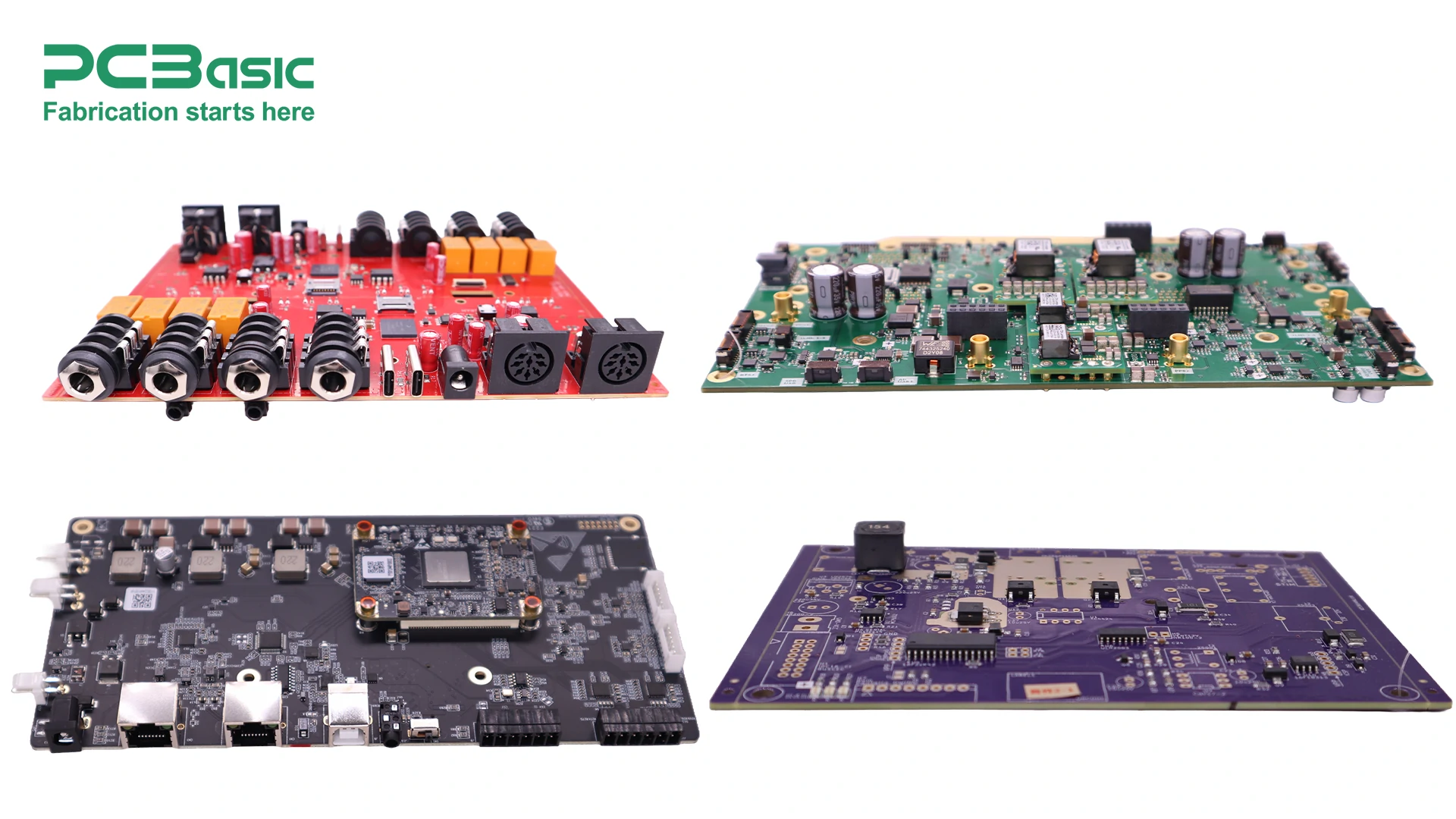
The main difference between bare PCB and PCBA (printed circuit board assembly) is their degree of completion and functionality.
After reading the above, we already know that the bare circuit board includes only conductive copper traces and pads, which is the basis of electronic component soldering. A bare PCB is the initial stage in the assembly process.
The PCBA is a circuit board that has completed component soldering, and all the necessary electronic components, such as resistors, capacitors, integrated circuits and connectors, have been soldered to the bare PCB. The assembly process includes the soldering and connection of components to turn the bare PCB into a complete functional circuit.
Here’s a comprehensive comparison of bare PCB vs PCBA:
|
Feature |
Bare PCB |
PCBA |
|
Definition |
A blank, unassembled printed circuit board |
A fully assembled PCB with all components soldered on |
|
Components |
No electronic components |
Fully populated with resistors, capacitors, ICs, etc. |
|
Functionality |
Non-functional (just the board) |
Fully functional and operational circuit |
|
Purpose |
Base structure for component assembly |
Complete and operational circuit ready for use |
|
Manufacturing Stage |
After fabrication, before assembly |
After assembly, testing, and quality check |
|
Applications |
Used in PCB manufacturing and assembly |
Used in end products like electronics, gadgets, and devices |
|
Cost |
Lower cost (due to fewer steps) |
Higher cost (due to assembly, testing, and final quality control) |
|
Surface Treatment |
May have surface treatments for solderability (e.g., HASL, ENIG, OSP) |
Fully treated and ready for final product integration |
In contrast to professionally manufactured bare PCBs, the zero PCB is a general-purpose circuit board commonly used in prototyping and DIY electronics projects. It has a regularly arranged grid layout with pre-drilled holes and copper pads at each grid point for users soldering and connecting components.
Unlike traditional professional PCBs, zero PCBs have no predefined circuit traces or electrical layout, and users are free to design and adjust circuit connections according to specific needs. By connecting the grid points with wires or solder, users can quickly build simple circuit prototypes. Due to its flexible design and ease of use, zero PCBs are ideal for rapid testing, electronic prototyping, and personal DIY projects.
|
Feature |
Zero PCB |
Bare PCB |
|
Design |
No predefined traces, flexible layout. |
Predefined design for specific use. |
|
Purpose |
Prototyping and DIY projects. |
Large-scale production and high performance. |
|
Structure |
Grid with pre-drilled holes and copper pads. |
Layered with traces, vias, and components. |
|
Reliability |
Manual assembly, less consistent. |
Automated, highly reliable. |
|
Users |
Hobbyists, students, DIYers. |
Professionals and industries. |
|
Cost |
Low for small projects. |
Cost-effective for mass production. |
If you are looking for a trusted partner for bare PCB manufacturing, PCBasic stands out as an industry leader. Keep reading, and you will believe that you will have an unforgettable cooperation experience with PCBasic.
PCBasic offers comprehensive services that go beyond bare PCB manufacturing, providing one-stop solutions that include PCB design, material selection, prototyping, assembly, and testing. This holistic approach ensures that customers receive complete support throughout the entire production process.
As an intelligent factory, PCBasic leverages state-of-the-art technologies to enhance efficiency and quality. With integrated CRM, MES, ERP, and IoT systems, the company streamlines operations and improves productivity. Advanced technologies, such as LCR incoming inspection and SMT fault detection systems, further reinforce the precision and reliability of our manufacturing processes.
Our bare PCB boards serve a diverse range of industries, including automotive electronics, medical devices, smart home systems, and communication power systems. These wide-ranging applications highlight the versatility and quality of PCBasic's offerings.
Certified to ISO9001, IATF16949, and ISO13485 standards, PCBasic maintains strict quality control processes to ensure every bare PCB meets the highest levels of excellence. This commitment to quality is supported by a team of over 30 skilled PCB designers and 20 quality management specialists, providing 24/7 customer support to address any needs.
With more than 15 years of industry experience, PCBasic continuously invests in innovation and PCBA technology, ensuring that every bare PCB board delivers unmatched performance and reliability. This dedication to expertise and innovation positions PCBasic as a leader in the PCB manufacturing sector.
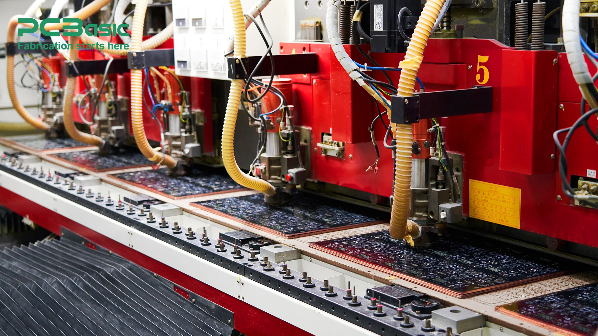
Bare board PCB is the starting point of any electronic device and provides the necessary framework for circuit assembly. If you are looking for a bare PCB manufacturer, contact PCBasic.
Assembly Enquiry
Instant Quote
Phone contact

+86-755-27218592
In addition, we've prepared a Help Center. We recommend checking it before reaching out, as your question and its answer may already be clearly explained there.
Wechat Support

In addition, we've prepared a Help Center. We recommend checking it before reaching out, as your question and its answer may already be clearly explained there.
WhatsApp Support

In addition, we've prepared a Help Center. We recommend checking it before reaching out, as your question and its answer may already be clearly explained there.