In this era of advanced technology, printed circuit boards (PCBs) serve as the foundation of the majority of gadgets we use and tented vias are one of its many attributes. Tented via is a design detail that is frequently found in PCB manufacturing.
This article aims to assist you in answering all of these questions. We intend to analyze defining tented vias along with their types, benefits, design considerations and attempts to compare to others via treatments like via plugging. By the end of this article, you will be well-versed in tented vias and how they ought to be treated within the PCB design process.
What is a Tented Via?
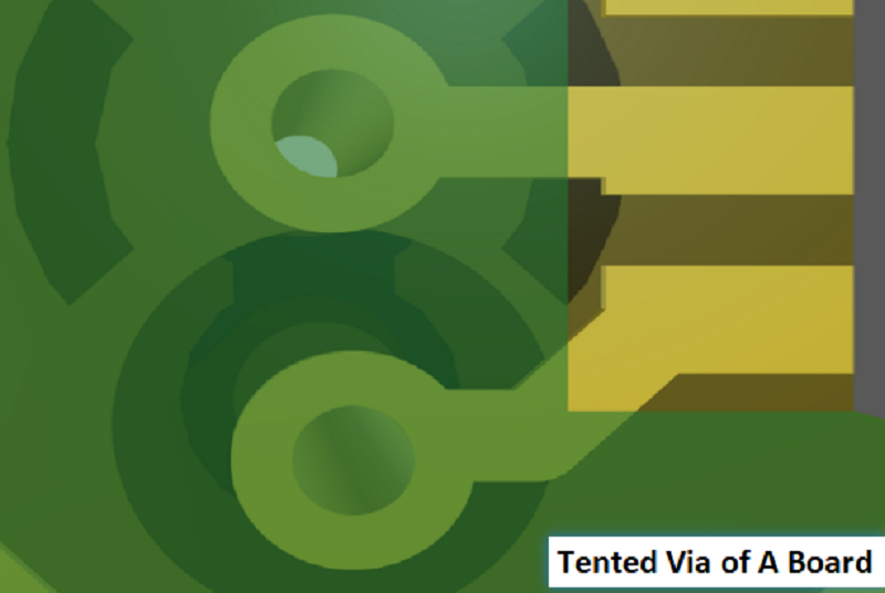
Tented vias are one type of vias with a particular feature in which the cover, or seal of the via, is covered by a solder mask material. A via is described as a hole that is made in the PCB for the purpose of connecting different layers of the board. Tenting is also done to improve the contamination control features of the via to maintain it free from dust, solder, and other contaminants during operational or assembly activities.
Tented vias are favorable with PCB designers as they are known to increase the PCB's reliability while reducing short circuit risks. Understanding how a tented via works is easier when one considers that a solder mask, or a mask that covers a via, is placed on top of the via. It is especially beneficial in the case of high-density PCB designs with space constraints as well as contamination and solder bridging issues.

Types of Tented Via
These are solder mask tented vias, which are fully covered, and partially covered copper tented vias.
Fully Tented Vias: They are completely masked and have no copper exposed, which helps possibly prevent contamination improving high-density PCB designs. Fully Tented Vias are usually found in consumer electronics, as they balance the need for good design with sound engineering.
Partially Tented Vias: In these cases, the copper is covered by a solder mask, but some remain exposed. It is useful in cases where electrical testing or rework is required. Partially Tented Vias are common in prototypes or industrial designs that need to be tested and debugged.
Advantages and Disadvantages
Advantages of Tented Vias:
1. Solder, dust, and moisture protection are the main advantages of tented vias, which consecutively improve the reliability of the PCB.
2. Such is the reality for the harsh environment of PCBs, the presence of contaminants is detrimental to performance which is why it is one of the most significant problems.
3. PCBs with clean and solder masks look professional, therefore, they not only fit consumer PCBs but also industrial electronics where appearance is crucial so it is able to earn Enhanced Appeal.
4. Accidental bridging or contact is reduced by covering the via. For densely packed designs with high component density, this is quite notable.
5. General purpose PCBs can easily be tented making them cheaper and economical. This is a lot cheaper than other via treatments like via plugging making it Saves Money.
Disadvantages of Tented Vias:
1. Achieving these fully tented vias means the mask has to be removed to debug them, making them impossible to reach. Hence, there is no option for rework.
2. Exposing the via after applying too much thickness on the solder mask can cause it to crack thermally during cycling, making it a risk of cracking on the solder mask. This causes less reliability over time.
3. Tent vias are generally not usable for applications like military or medical devices because they are of very high reliability making them not for certain applications.
Key Parameters and Specifications for Vias
A few key details associated with tented vias are of special focus to accomplish the best performance:
Via Diameter- This refers to the size of the hole made on the circuit board and how wide it can be tented. Smaller vias are easier to cover, while larger vias might need thicker layers of solder masks to guarantee total coverage. Tent larger vias may be challenging. Smaller vias can be difficult to drill.
Aspect Ratio- This is normally expressed as the diameter of a given via to its depth. Via tenting masks are very difficult to achieve at higher aspect ratios, but it is not best to go too much beyond the limit set by the manufacturer.
Solder Mask Thickness- Within limits that are too thick or too thin, the layer of the solder mask can crack or be inadequately covered. Too little in the sense, does not support the protection required for the via, while too much thickness can suffer from cracking during thermal cycling.
Material Compatibility- The solder shield has to be compatible with the PCB's substrate, but it has to survive the assembly for the unit.
Epoxy resin and liquid photoimageable (LPI) solder masks are some of the commonly used solder mask materials.
Design Considerations for Via Tenting
When via tented are being created, the tented vias layout has to conform with the PCB specifications. The functions which need to be fulfilled must be compatible with the aesthetic elements of the device. The following are some considerations for tented via PCB designs:
Placement of the Via: Tented vias are recommended to be located in more passive regions so as not to facilitate damage to the solder mask. As an illustration, avoid placing vias at the corners of the Printed Circuit Board (PCB) or within regions subjected to Mechanical loading.
Solder Mask Application: Apply the covering layer of the solder mask with sufficient and consistent coverage, free from voids or low coverage areas. If a mask is not applied correctly, the coverage may not be enough, and therefore, this mask will not function as tented via will be limited.
Thermal Management: Include consideration of the potential thermal expansion of cracks induced by softening or cooling a solder mask. This is critical for PCBs which are going to be exposed to extremely high or low temperatures.
Testing needs: If there will be electrical testing, it may be beneficial to make partially tented vias so that the via will be accessible. The presence of fully tented vias complicates many testing and troubleshooting tasks, particularly concerning the tenting and dismounting phases of the accommodation.
Manufacturing Processes: All PCB manufacturers must be examined to determine what their limitations are concerning the tented via
Some manufacturers could hold some restrictions regarding the minimum dimensions, aspect ratio of the vias, or the maximum thickness of the solder mask.
Tented Via vs. Via Plugging
What is Via Plugging in PCB?
Traditional plugging designs have at least one through via holes that are either filled with a conductive or non-conductive material used for plugging. Plugging is one of the specialized via treatments in PCB design. By providing non-conductive plugging, some structural support can be provided while preventing the solder from wicking away during assembly. Plugging can be found common in aerospace, automotive, and a few medical devices where reliability is usually a concern.
Tented Via vs. Via Plugging (Compare Table)
|
Feature
|
Tented Via
|
Via Plugging
|
|
Protection
|
Protects against contaminants
|
Provides structural support
|
|
Material
|
Solder mask
|
Conductive or non-conductive fillers
|
|
Cost
|
Lower cost
|
Higher cost
|
|
Reworkability
|
Limited for fully tented vias
|
Easier due to the filled structure
|
|
Applications
|
General-purpose PCBs
|
High-reliability or high-density PCBs
|
|
Thermal Performance
|
May crack under thermal stress
|
Better thermal stability
|
|
Aesthetics
|
Clean and professional appearance
|
May leave visible filler material
|
Via Tenting Manufacturing Process
Processes of Tented Vias manufacturing come to the following steps:
Drilling- The Vias are drilled as per the drawing. Like all Vias, the size and location of the vias are critical to proper via tenting.
Plating- In this step, copper plating is done on the vias to make an electric connection with other layers of the PCB. This also provides additional support to the structure of the via.
Application of Solder Mask- A solder mask is used on the whole PCB and it also plugs the vias. Screen printing or spray coating methods are applied to the mask.
Curing- The mask is cured, which is a pre-step of hardening. The curing procedure utilizes either heat or UV lasers to irradiate the solder mask depending on its type.
Inspection- Every PCB goes through an inspection where the closed vias are analyzed for the ability of the 'tent' function to cover the vias. AOI is an excellent void detection tool for incomplete coverage such as voids or cracks, and monitors it extremely effectively.
This method guarantees that the closed vias will keep the functionality while providing enough coverage.
Applications of Tented Vias
Due to their low cost and reliability, tented vias are used in many different sectors. These include:
Consumer Electronics- Tablets, smartphones, and laptops can take advantage of tented vias as the exposed surface is free of contaminants, preserving the aesthetic.
Automotive Electronics- Tented vias are widely used in automotive PCBs as they can survive harsh environments that may lead to dust or moisture short-circuiting.
Industrial Equipment- Tented vias assist controls and machinery that are susceptible to contaminating failures.
LED Lighting- Tented vias improve the reliability and performance of the high-temperature LED PCBs.
Challenges in Tented Via Manufacturing
Although the purpose of tented vias is rather limited, there are issues related to its fabrication:
Poor Adhesion- Depending on the size and aspect ratio, the presence of tented vias can cause the die solder mask to fail, leading to poor adhesion.
Thermal Cracking- During temperature cycling, the contraction and expansion of the solder mask causes it to crack or delaminate.
Incomplete coverage- An overexposed via concealed mask due to poor solder mask application.
Process Control- For mass production, tighter control over the processes is needed to achieve consistency via tenting, which leads to coverage uniformity.
Future Trends in Via Tenting
With the evolution of new technologies in the PCB industry, via tenting PCB is bound to evolve. Some may include:
Better Mechanical Solder Mask Materials- New solder masks that provide better mechanical and thermal performance will render tented vias more reliable.
Laser-Assisted Tenting- A more uniform and precise application of the solder mask making use of lasers is called Laser-Assisted Tenting.
Hybrid Via Treatments- Also referred to as tenting vias in conjunction with procedures like via filling, for improved performance in high-reliability applications.
Automated Inspection Systems- New AOI systems are being built with the capability to rapidly and accurately identify defects found in tented vias.
Conclusion
Presently, tented vias in PCB layouts provide aesthetic value, improved obstruction to contaminants, and reduced probability of short circuits. Knowing the various classifications of tented vias and their advantages, along with other design issues, equips one better for PCB design assignments.
When comparing general-purpose PCBs, tented vias are less expensive than plugging vias, although the latter is more appropriate for high-reliability applications. In either case, whether employing tented vias or plugging vias, the most important considerations in the decision process need to be the design requirements and factory production capabilities of the plasterboard design center. Designing a PCB with tented vias increases the reliability and performance of electrical appliances. For the tented vias or any other requirements regarding PCB manufacturing, seek guidance from specialized PCB manufacturers.