Global high-mix volume high-speed PCBA manufacturer
9:00 -18:00, Mon. - Fri. (GMT+8)
9:00 -12:00, Sat. (GMT+8)
(Except Chinese public holidays)
Global high-mix volume high-speed PCBA manufacturer
9:00 -18:00, Mon. - Fri. (GMT+8)
9:00 -12:00, Sat. (GMT+8)
(Except Chinese public holidays)
HomePage > Blog > Knowledge Base > Understanding PCB Shielding
Do you know what PCB shielding is? Today, let's learn about "PCB shielding"!
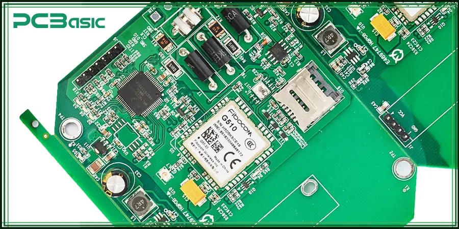
In modern electronic equipment, wireless communication speed is increasing, the system function is becoming more and more complex at the same time, accompanied by a problem that can not be ignored - electromagnetic interference (EMI). Electromagnetic interference can affect the signal integrity and electromagnetic compatibility of electronic devices; While signal integrity and electromagnetic compatibility, in turn, are critical for high-frequency, compact electronic systems such as smartphones, automotive control modules, and communication interfaces in industrial equipment. Therefore, in order to solve this problem, PCB shielding (EMI protection method) is needed. PCB shielding is an indispensable design method for electronic engineers to ensure stable circuit performance, reliable data transmission, and meet various EMC (electromagnetic compatibility) certification standards.
Next, this article will take you to a comprehensive understanding of PCB shielding techniques: from the principle of PCB shielding, type (such as board level, level, line level, device level, etc.), to material selection, design points, and its practical application in RF communication, automotive electronics, medical equipment and industrial control. Let's have a look!
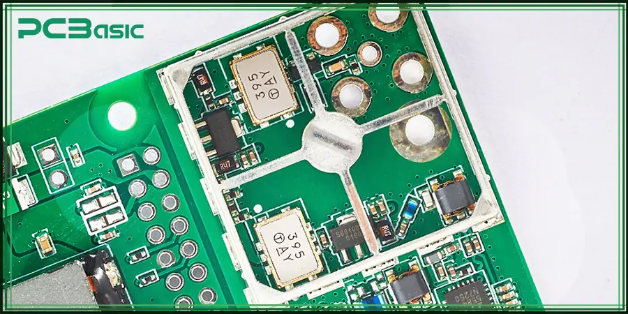
PCB shielding refers to a technology that blocks or reduces electromagnetic interference (EMI) in electronic circuit boards by physical, electrical or material means, which can both suppress the interference emitted by PCB and prevent external interference signals from entering the circuit system. In modern electronic systems, especially applications involving high-speed signals or radio frequency (RF) signals, PCB EMI shielding plays a vital role in maintaining signal integrity and ensuring electromagnetic compatibility (EMC).
In essence, shielding PCB by the addition of conductive barriers, such as PCB shielding cans, shielding covers, ground planes or metal shells, Isolate sensitive devices or wires from noise sources (these barriers absorb or reflect unwanted electromagnetic energy, thereby preventing interference from affecting circuit performance). Effective PCB EMI shielding can improve electromagnetic compatibility (EMC) and is an indispensable part of modern circuit board shielding design.
Efficient PCB shielding preserves signal integrity by isolating sensitive wiring and components from internal or external noise sources. It also plays a key role in meeting global electromagnetic compatibility standards such as FCC, CE, CISPR, which are essential for compliance with the vast majority of commercial electronic products.
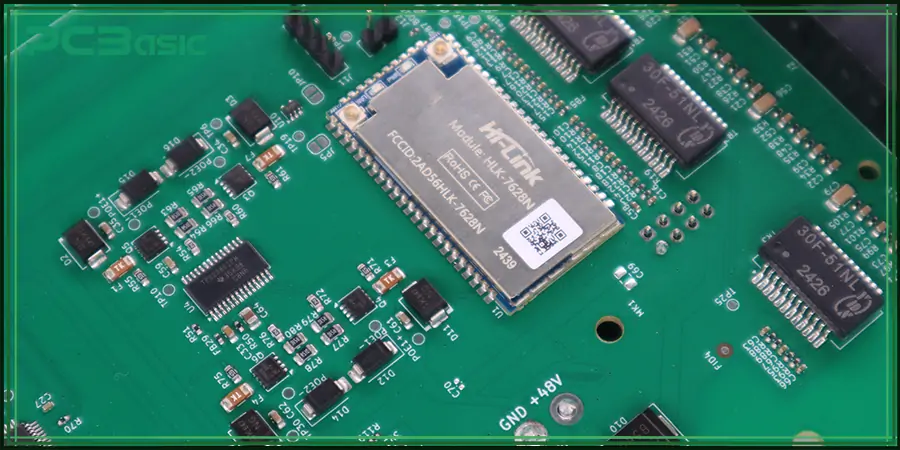
In addition, in PCB RF shielding applications, the shielding design is particularly critical because high-frequency signals are highly susceptible to interference. Through the reasonable application of PCB shielding technology (such as shielding cans, ground planes, shield traces, etc.), the stability of the product can be significantly improved, the service life can be extended, and the certification process can be accelerated. Effective PCB EMI shielding design improves system stability, functional safety, and certification success.
Electromagnetic Interference (EMI) is the undesired electromagnetic energy that interferes with the normal operation of electronic circuits. These disturbances may come from internal sources (such as switching regulators, high-speed data signal lines) or external sources (such as power lines, wireless transmitters, etc.). EMI can degrade signal quality, cause data errors, and even cause the failure or failure of sensitive components.
Electromagnetic Compatibility (EMC) is the ability of a device to function properly in its electromagnetic environment without causing interference to other devices. In order to achieve EMC, effective PCB EMI shields design is required.
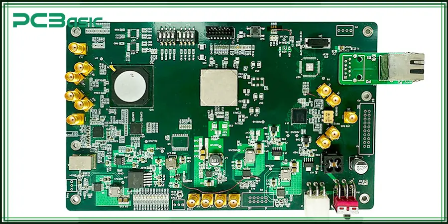
The types of PCB shielding are various, and I will introduce you from the aspects of board-level shielding, wire-level shielding, level shielding and device-level shielding.
Board level shielding is one of the most widely used EMI protection methods. It is achieved by covering the sensitive areas of the board with PCB shielding cans, metal shielding covers or PCB shielding enclosures . These barriers physically isolate high-frequency areas, effectively preventing EMI from radiating outward or coupling into the surrounding circuit.
Common ways include:
This approach enables robust PCB EMI shield, which is widely used in wireless communications, IoT and radar systems.
Trace level shielding is primarily used to protect high-speed signal traces, achieving EMI isolation by adding shield trace, guard trace, or filling ground layers around critical networks. In PCB EMI shielding design, microstrip and stripline are also commonly used to control impedance and reduce radiation.
By adding grounded shielding wires next to the data signal, crosstalk can be greatly reduced and signal quality can be improved for high-speed digital circuits and RF PCB shielding systems.
Layer shielding enables in-board integrated PCB shields by embedding ground planes or shields in the PCB stack structure. These inner shields provide a low impedance return path that effectively inhibits EMI propagation.
This type of PCB level shielding is especially suitable for multi-layer circuit board designs, and it can significantly improve the overall EMI shielding PCB effect by sandwiching the layer on both sides of the critical signal.
Where local EMI protection is required, component-level shielding is applied to specific components, such as ICs, RF chips, power modules, etc. Such methods include:
These PCB shielding technologies are particularly important in high-density layouts and can effectively isolate the interference problems caused by the coexistence of multiple noise sources.
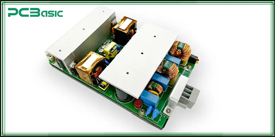
In the design of PCB shielding, we must choose the right shielding material. Only the right PCB shielding material can play a good role in the suppression effect of electromagnetic interference. Different materials vary in conductivity, corrosion resistance, weight, cost, and manufacturability. Understanding these material properties can lead to a more efficient and cost-effective PCB EMI shielding solution.
|
Material |
Properties |
Application Advantages |
|
Copper |
High conductivity, excellent EMI shielding |
Ideal for high-performance RF PCB shielding, though relatively high in cost |
|
Aluminum |
Lightweight, good conductivity, cost-effective |
Suitable for mass production, widely used in PCB shielding cans and enclosures |
|
Nickel Silver Alloy |
Corrosion-resistant, highly processable |
Used in complex structures or harsh environments, ideal for PCB shielding enclosures |
|
Conductive Fabric |
Flexible, lightweight, easy to attach |
Suitable for flexible circuits or lightweight devices such as wearables |
|
Conductive Tape |
Easy to apply, suitable for temporary shielding |
Ideal for prototyping, EMI troubleshooting, or low-volume production |
Designing an effective circuit board shield requires consideration of several factors:
1. Reasonable arrangement of shielding covers and shielding covers: the PCB shielding cans or shielding covers are directly covered on key devices (such as RF modules, crystal oscillators, high-speed ICs, etc.), which should leave enough space for heat dissipation and later maintenance. And unless there is a special need, it is necessary to avoid excessive proximity of the shield to the passive device.
2. All PCB shielding structures must have a low-impedance grounding path. It is recommended to use via stitching around the PCB shield cover to enhance grounding continuity. Avoid using long and thin lines to connect the PCB shield to the ground, because this type of structure is easy to become an antenna, but will amplify the interference.
3. If there is a gap or discontinuous area in PCB level shielding, it will become an EMI leak point, so be sure not to leave gaps and loops in the shielding structure.
4. It is recommended to arrange shield trace or guard trace around high-speed signals to effectively converge interference and provide a stable return path.
5. Physically isolate high-noise circuits such as switching power supplies and radio frequency transmitters from analog or high-speed digital circuits. At the same time with the use of EMI protection methods, such as filters, magnetic beads and other components to enhance the overall shielding effect.
6. Ensure that the PCB shielding techniques selected do not affect thermal performance or create mechanical stress. If necessary, a shielding cover with a vent can be used to ensure smooth air circulation.
The application of PCB shielding is also very wide. Below, I will focus on the application of PCB shielding in RF communications, automotive electronics, medical devices, and industrial control.
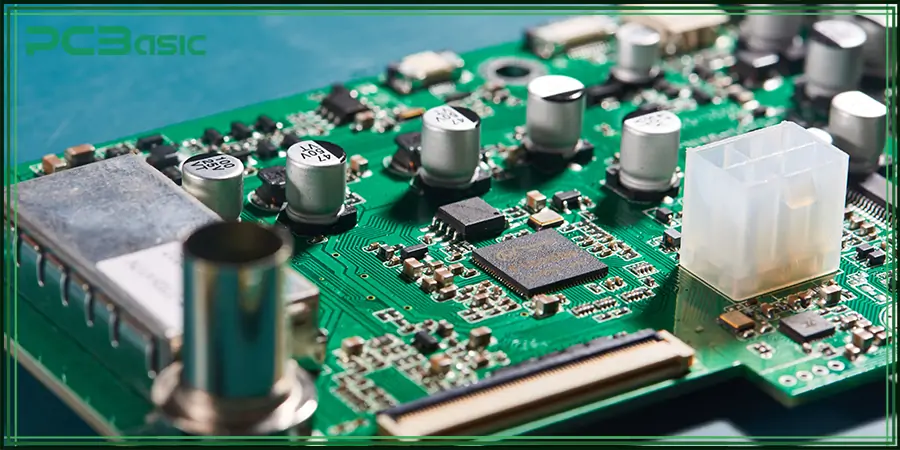
In RF communication, such as wireless base stations, Wi-Fi modules, GPS devices, 5G antennas, etc., the signal frequency is high, the transmission distance is long, and the electromagnetic interference (EMI) is extremely sensitive.
In RF communication, PCB shielding mainly uses PCB shielding cans to protect RF modules (such as LNA, PA, VCO). The signal crosstalk is suppressed by shield trace and strip structure. And the ground layer will be added in the multi-layer board design as the RF signal shielding barrier. Metal enclosures or Faraday cages are often used throughout the module to achieve complete RF PCB shielding.
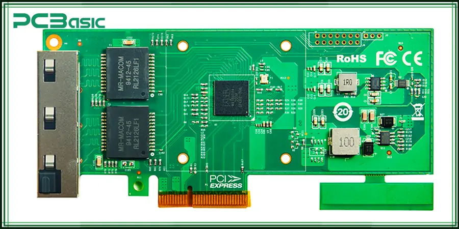
In modern automobiles, electronic control units (ECUs), radar, vehicle communication modules, ADAS systems and other equipment are widely used in strong current and electromagnetic complex working environments. In order to ensure that the key electronic system has strong anti-interference ability and ensure the driving safety and the reliability of the vehicle system, PCB shielding is also essential.
The key points of PCB shielding in automotive electronics are:
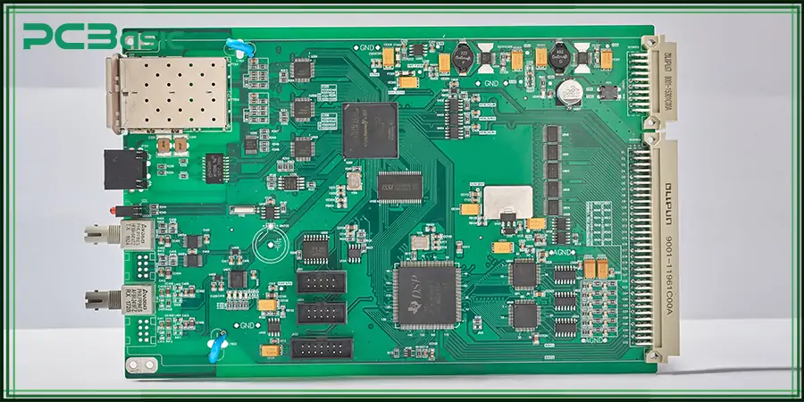
The accuracy and stability of the signal requirements of medical devices are extremely high, such as electrocardiogram (ECG), MRI, ultrasound, wearable medical devices, etc.. Once received EMI interference will affect the diagnostic results. Therefore, in order to ensure diagnostic accuracy, data transmission security, and medical grade EMC certification (such as IEC 60601-1-2), PCB shielding is required.
For example, the shielding PCB structure is used to protect the front-end signal of the sensor; Use flexible conductive material or conductive cloth for external interference isolation; RF PCB shielding design is adopted for high-frequency signal processing unit to shield high-frequency noise; Independent metal cover partition shielding is used between modules to prevent internal interference.
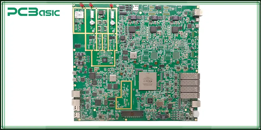
PCB shielding is also required for industrial control systems. Such as PLC, industrial control motherboard, frequency converter, servo drive and other equipment are often deployed in industrial environments with serious electromagnetic interference (such as high-voltage computer rooms, substations or large-scale automated production lines, etc.). In this environment, PCB shielding is required to maintain the stable operation of the equipment.
In industrial control systems, metal shielding boxes and multi-point grounding structures are used in high-frequency and high-power equipment; The precision control unit uses PCB EMI shielding design to reduce inductive interference; Multi-layer PCB structure is used to realize signal isolation and power layer isolation. Isolation strips and shielding lines are set up between analog and digital circuits. These are good ways to improve the anti-interference ability of the system, reduce the failure rate, and improve the stability and durability of the industrial control system.
Whether developing RF shielding PCBs, automotive electronics PCBs, medical devices, or other devices, shielding design should be a key part of the development process. PCB shielding is not only used for compliance, but also to improve the performance and reliability of your equipment. PCB shield design should be considered from the early stage of product development. Incorporating shielding design considerations at the beginning of the design ensures a more coordinated design of the entire system and reduces the need for later corrections, which contributes to cost control throughout the development process.

Assembly Enquiry
Instant Quote
Phone contact

+86-755-27218592
In addition, we've prepared a Help Center. We recommend checking it before reaching out, as your question and its answer may already be clearly explained there.
Wechat Support

In addition, we've prepared a Help Center. We recommend checking it before reaching out, as your question and its answer may already be clearly explained there.
WhatsApp Support

In addition, we've prepared a Help Center. We recommend checking it before reaching out, as your question and its answer may already be clearly explained there.