Global high-mix volume high-speed PCBA manufacturer
9:00 -18:00, Mon. - Fri. (GMT+8)
9:00 -12:00, Sat. (GMT+8)
(Except Chinese public holidays)
Global high-mix volume high-speed PCBA manufacturer
9:00 -18:00, Mon. - Fri. (GMT+8)
9:00 -12:00, Sat. (GMT+8)
(Except Chinese public holidays)
HomePage > Blog > Knowledge Base > What Are PCB Mounting Holes?
A printed circuit board (PCB) is a crucial component in electronic equipment, providing a platform for the installation and connection of electronic components. Different PCBs vary in shape, size, and design according to equipment requirements. The development of PCBs has enabled electronic devices to become miniaturized, lightweight, and cost-effective for mass production.
However, an often-overlooked yet essential feature in PCBs is the PCB mounting hole. These small yet critical PCB mounting holes allow the PCB to be securely attached to the enclosure or device, ensuring the stability of electronic component installation and protecting the circuit from mechanical stress. Proper PCB mounting is crucial in ensuring long-term performance, especially in environments prone to vibration or movement.
In this blog, we will discuss what PCB mounting holes are, their types, and how they differ from via holes on a PCB. Understanding the importance of PCB mounting hole size and selecting the correct M3 clearance hole or non-plated through hole will ensure stability in your design.

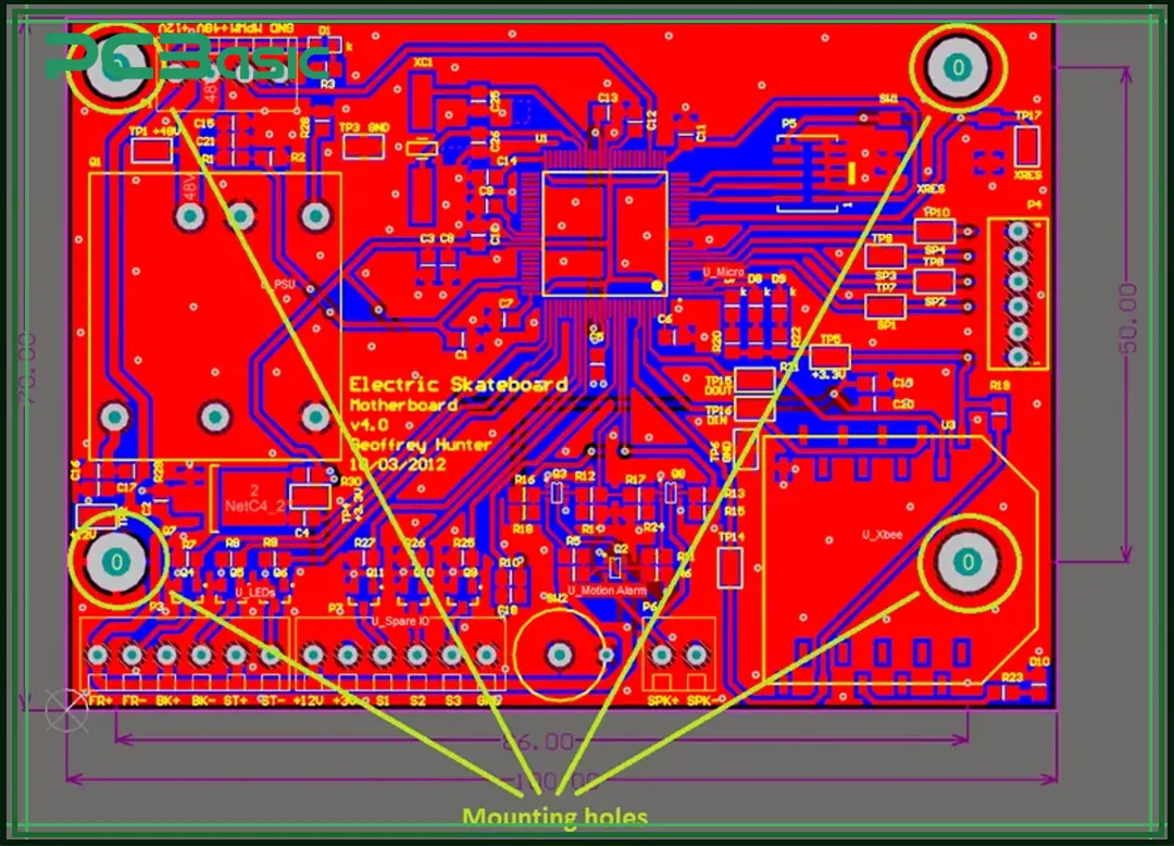
PCB mounting holes are small round holes in the printed circuit board, usually located in the corners or edges of the PCB, ensuring that the board is securely fixed.
The PCB mounting hole has two main functions:
One is physical fixation.
The PCB mounting hole provides a mounting point for the physical installation of the PCB. By inserting screws or other fixing devices into the mounting holes, the PCB can be securely installed on the shell or bracket of the device. This can prevent the circuit board from being affected by external forces such as movement and vibration during use and ensure its normal operation. Choosing the correct PCB mounting hole size is key to achieving stable mounting.
The second is electrical grounding.
In some circuit designs, mounting holes can also be used for electrical grounding. This means that through these holes, PCBs can be connected to device shells or other conductive parts. This can help the circuit to achieve a stable potential reference, reduce electromagnetic interference and improve the efficiency and safety of the circuit.
Unlike other types of holes on the PCB, such as through-holes for electrical connections, PCB mounting holes do not transmit electrical signals. They are usually aligned with the design of device shells or other components that fix PCBs.
The size of PCB mounting holes can vary depending on the specific design requirements, the type of fasteners or screws used, and the overall dimensions of the board. Here’s a general s PCB mounting hole size chart for common screw sizes:
|
Screw Size |
Hole Diameter (mm) |
Hole Diameter (inches) |
|
M2 |
2.2 - 2.4 mm |
0.086 - 0.094 inches |
|
M2.5 |
2.7 - 2.9 mm |
0.106 - 0.114 inches |
|
M3 |
3.2 - 3.4 mm |
0.126 - 0.134 inches |
|
M4 |
4.3 - 4.5 mm |
0.169 - 0.177 inches |
|
M5 |
5.3 - 5.5 mm |
0.209 - 0.217 inches |
|
#4-40 (Imperial) |
3.0 - 3.2 mm |
0.118 - 0.126 inches |
|
#6-32 (Imperial) |
3.5 - 3.8 mm |
0.138 - 0.150 inches |
The M3 clearance hole is one of the most common sizes used in PCB designs, offering secure fastening while ensuring the right fit for mechanical strength.
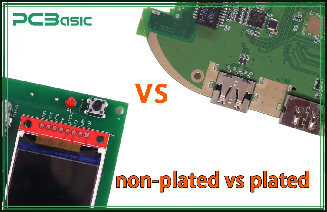
Due to different design and manufacturing requirements, we can divide PCB mounting holes into two types according to whether they are plated: plated mounting holes and un-plated mounting holes.

Plated mounting holes are drilled holes on a PCB that have been coated with a thin layer of conductive material, usually copper, around their inner circumference.
Plated mounting holes are commonly used when the mounting process requires grounding the PCB to the enclosure or other conductive parts. They offer added strength and improved stability, especially when using M3 clearance hole screws for secure mounting.
Un-plated mounting holes, also known as non-plated through holes, lack a conductive coating on their inner surface. These holes are strictly mechanical, serving only as physical attachment points. They are common in designs where no electrical grounding is required. Choosing a non-plated through hole is often a more cost-effective option for securing PCBs without compromising mechanical strength.
Here is a comprehensive comparison between plated mounting and un-plated mounting holes:
|
Feature |
Plated Mounting Holes |
Un-plated Mounting Holes |
|
Conductive Coating |
Has conductive coating (copper) |
No conductive coating |
|
Electrical Grounding |
Yes, can be used for grounding |
No, purely mechanical |
|
Structural Strength |
Stronger due to copper plating |
Weaker compared to plated holes |
|
Manufacturing Cost |
Higher due to plating process |
Lower, no plating required |
|
Design Complexity |
More complex, requires additional considerations |
Simpler, no electrical considerations |
There are many different types of holes on a PCB, including mounting holes, via holes, component holes, test points and alignment holes. Each of these holes plays a vital role in both the physical structure and electrical functionality of the PCB.
Among them, mounting holes and via holes are the most common holes and people always confuse them. Therefore, it is essential to distinguish the two on a PCB, as they serve entirely different functions, despite both being holes drilled into the PCB.

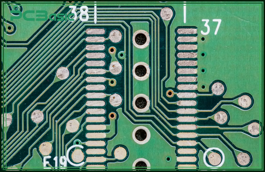
Via holes are an integral part of the PCB’s electrical design. They allow for the transfer of electrical signals between different layers of the board. In multi-layer PCBs, vias enable connections from surface traces or components to inner-layer circuits, ensuring that electrical signals are routed correctly throughout the board.
Vias are typically much smaller than mounting holes and are filled or plated with conductive material, such as copper, to allow signal transmission.
On the other hand, mounting holes do not carry electrical signals. Their primary function is mechanical: they are used to secure the PCB to a surface or enclosure. While via holes play a crucial role in the electrical operation of the circuit, mounting holes do not, except in specific cases where plated mounting holes are used for grounding purposes.
|
Feature |
Mounting Holes |
Via Holes |
|
Purpose |
Mechanical, sometimes grounding |
Electrical signal routing between PCB layers |
|
Size |
Larger to accommodate screws or fasteners |
Smaller, designed to fit signal paths |
|
Plating |
Can be plated or un-plated |
Always plated for electrical conduction |
PCB mounting holes may seem minor, but they are vital in ensuring the durability, functionality, and reliability of electronic devices. Without proper PCB mounting, even the most sophisticated designs could fail due to mechanical stress, vibration, or heat expansion. By carefully designing and implementing PCB mounting holes, you can achieve stable and effective PCB installations.
Whether you require an M3 clearance hole, a precise PCB mounting hole size, or a reliable PCB mounting hole size chart, understanding these key factors will help you create robust PCB designs. Pay attention to plated and non-plated through hole options to ensure the best performance for your electronic projects.

Assembly Enquiry
Instant Quote
Phone contact

+86-755-27218592
In addition, we've prepared a Help Center. We recommend checking it before reaching out, as your question and its answer may already be clearly explained there.
Wechat Support

In addition, we've prepared a Help Center. We recommend checking it before reaching out, as your question and its answer may already be clearly explained there.
WhatsApp Support

In addition, we've prepared a Help Center. We recommend checking it before reaching out, as your question and its answer may already be clearly explained there.