Global high-mix volume high-speed PCBA manufacturer
9:00 -18:00, Mon. - Fri. (GMT+8)
9:00 -12:00, Sat. (GMT+8)
(Except Chinese public holidays)
Global high-mix volume high-speed PCBA manufacturer
9:00 -18:00, Mon. - Fri. (GMT+8)
9:00 -12:00, Sat. (GMT+8)
(Except Chinese public holidays)
HomePage > Blog > Knowledge Base > Microstrips in High-Frequency PCB Design
As electronic devices advance in speed and complexity, the design of high-frequency printed circuit boards (PCBs) has become very important. In the design of various signal transmission lines, microstrip has become one of the most commonly used choices because of its simple structure and good performance.
In this blog, let’s explore the main information about PCB microstrips:
Structure of a microstrip line
Key characteristics of microstrips
Applications of microstrips
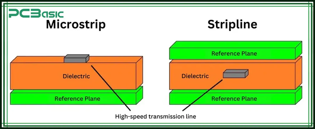
Microstrip vs. stripline
In short, if you want to design high-speed, efficient circuit boards, understanding the characteristics and application scenarios of microstrip lines is key.
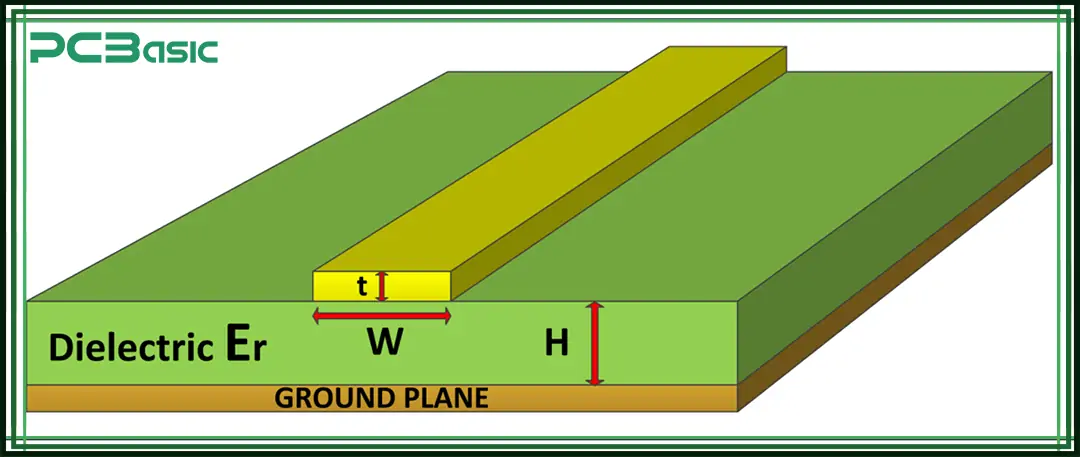
The microstrip line is an electrical transmission line commonly used in PCBs for transmitting high-frequency or RF signals. Its structure is very simple, mainly composed of three layers:

1. At the top, there is a slender conductive metal line, usually made of copper, which is the "highway" for signal transmission;
2. The middle layer is a dielectric material (such as FR-4 or other high-frequency materials), providing insulation;
3. At the bottom, it is a ground plane that provides reference potential and return path.
The structure is like a “sandwich,” with the signal flowing through the top trace, while the electromagnetic field partially passes through the dielectric layer below and partially spreads into the air. This means the electric field doesn’t propagate entirely within the dielectric. It is a hybrid transmission line, transmitting "half in the air, half in the dielectric."
For this reason, the signal propagation speed and characteristics of a microstrip are influenced by both media — air and the dielectric layer. This mixed propagation means we can't describe its electrical properties using a single dielectric constant. Instead, we use an effective dielectric constant to account for the combined effects.
The value of this effective dielectric constant directly affects the microstrip impedance, which in turn determines whether the signal can be transmitted reliably. Therefore, during the design process, engineers must perform microstrip impedance calculation using formulas or simulation software to ensure proper impedance matching and avoid signal reflection or distortion.

• εr: Dielectric constant of the substrate material (e.g., FR-4 ≈ 4.5)
• H: Height (thickness) of the dielectric between the trace and the ground plane
• W: Width of the microstrip trace
The geometry of the line—conductor width, dielectric thickness, and substrate material—determines the microstrip impedance. Calculating this impedance correctly is essential to prevent signal loss and ensure proper signal integrity. Various online tools can assist with microstrip impedance calculation, taking into account the effective dielectric constant.
Microstrips are widely used in high-frequency circuit design, mainly because they have many advantages in terms of manufacturing, structure, cost and application flexibility.
• Simple fabrication:
Compared with other complex transmission lines, the microstrip only requires a signal line on the top layer of the PCB and a continuous ground plane on the bottom layer. The middle is isolated by a layer of dielectric material. The entire structure does not require multilayer stacking or other special packaging processes, which greatly simplifies the PCB production process and is suitable for mass production.
• Compact size:
Microstrips occupy only one signal layer and one ground layer of the PCB, it saves more vertical space than embedded transmission lines such as striplines. This is particularly important in the context of the miniaturization of modern devices. Especially in applications with extremely high space requirements such as mobile phones, satellite modules, and on-board systems, microstrips become the ideal choice.
• Low cost:
Due to its fewer layers, simple structure, and low processing equipment requirements, the overall manufacturing cost of a PCB microstrip is much lower than that of multilayer packaging or embedded structures. This makes it particularly suitable for cost-sensitive products such as consumer electronics, IoT devices, and mid - and low-frequency RF modules.
• Supports complex circuits:
The microstrip can not only transmit high-frequency signals, but also flexibly build common RF functional modules such as power dividers, couplers and microstrip filter. Its ability to implement these functions in a flat structure makes circuit designs more compact and easier to lay out.
Therefore, many engineers tend to choose the microstrip, especially when there is no need for extremely high isolation or low EMI. Its advantages of convenient manufacturing, flexible layout and controllable cost make it a more cost-effective solution in practical engineering.

Although a microstrip has many advantages, it also has some limitations:
• Radiation losses: Signals are partially exposed to air, increasing EMI.
• Signal integrity: Sensitive to changes in substrate and temperature.
• Lower isolation compared to stripline designs.
Microstrip lines are used across a wide range of RF and microwave applications, including:
• Microstrip filters for signal conditioning
• Patch antennas for wireless communication
• Impedance-matched transmission lines
• Radar and satellite systems
A stripline is a commonly used routing structure in multilayer PCBs. Unlike a microstrip, a stripline places the signal trace between two ground planes, fully surrounded by a dielectric material, to form a symmetrical structure. This design helps reduce interference and noise, improving signal integrity—making it especially suitable for high-speed or high-frequency signal transmission.

The microstrip vs stripline comparison often arises during PCB design. Let’s compare the two in a table:
|
Feature |
Microstrip |
Stripline |
|
Signal Layer |
Top |
Embedded between two ground planes |
|
Field Propagation |
Air + Dielectric |
Entirely in Dielectric |
|
Effective Dielectric Constant |
Lower (Hybrid field) |
Higher (Fully dielectric) |
|
EMI Susceptibility |
Higher |
Lower |
|
Fabrication |
Easier |
More Complex |
|
Cost |
Lower |
Higher |
|
Application |
High-frequency, cost-sensitive |
High-precision, high-isolation |
In high-frequency PCB design, the microstrip plays a crucial role due to its simple structure, versatile applications, and controllable impedance. While there's no definitive answer in the microstrip vs stripline debate, PCB microstrip offers a practical balance between performance and manufacturability, making it a preferred choice in many applications.

Assembly Enquiry
Instant Quote
Phone contact

+86-755-27218592
In addition, we've prepared a Help Center. We recommend checking it before reaching out, as your question and its answer may already be clearly explained there.
Wechat Support

In addition, we've prepared a Help Center. We recommend checking it before reaching out, as your question and its answer may already be clearly explained there.
WhatsApp Support

In addition, we've prepared a Help Center. We recommend checking it before reaching out, as your question and its answer may already be clearly explained there.