Global high-mix volume high-speed PCBA manufacturer
9:00 -18:00, Mon. - Fri. (GMT+8)
9:00 -12:00, Sat. (GMT+8)
(Except Chinese public holidays)
Global high-mix volume high-speed PCBA manufacturer
9:00 -18:00, Mon. - Fri. (GMT+8)
9:00 -12:00, Sat. (GMT+8)
(Except Chinese public holidays)
HomePage > Blog > Knowledge Base > NMOS vs. PMOS: A Comprehensive Comparison
Metal-Oxide-Semiconductor Field-Effect Transistors (MOSFETs) have become fundamental as the building blocks of digital and analog circuits in modern electronics. MOSFETs can be further classified into two main types: NMOS (N-channel MOSFET) and PMOS (P-channel MOSFET), with each type exhibiting different properties and use cases. It is important to understand their differences in developing effective circuits, and in CMOS (Complementary Metal-Oxide-Semiconductor) technology they are also logically combined.
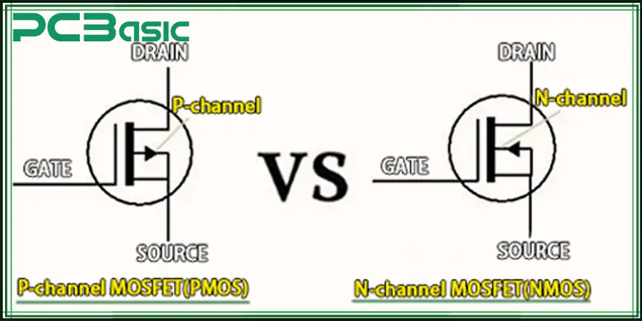
This guide will walk you through the NMOS vs PMOS with their symbols, direction of current flow, threshold voltages, structure, working and, applications.
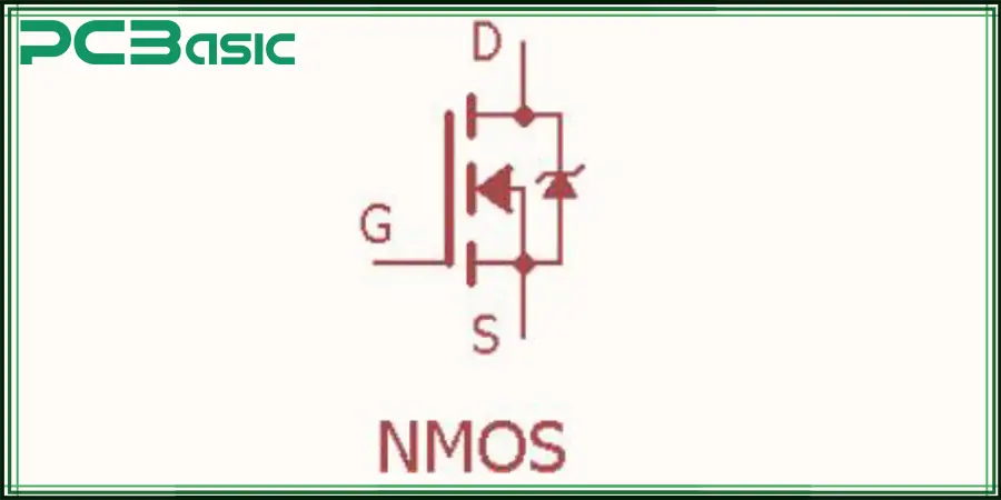
NMOS (N-channel MOSFET): A form of MOSFET, which contains n-type semiconductor material in the channel. If the gate voltage is applied then current flows.
PMOS (P-channel MOSFET ): A MOSFET built with a p-type or p-channel. It does conduct in response to negative gate voltage (less than a threshold).

The body effect is the effect of a (reverse) bias between the source junction and the body (or substrate terminal) leading to a change in threshold.
· In NMOS, the threshold voltage increases when the body is at a lower voltage than the source.
· This means that if for PMOS, the body is at a higher voltage than the source, the threshold voltage becomes more negative.
NMOS:
· Source and Drain: N-doped regions.
· Substrate (Body): P-doped.
· Gate (G): Controls channel formation.
PMOS:
· D (Drain) & S (Source): P-doped areas.
· Substrate (Body): N-doped.
· Gate (G): Channels Information Formation.
|
ASPECT |
NMOS |
PMOS |
|
Symbol |
Only inverse arrow (source to body). |
Arrow pointing outward (From body to source). |
|
Current Flow |
Electrons (majority carriers). |
Holes (majority carriers). |
|
Threshold Voltage |
Positive (e.g., +0.7V). |
Negative (e.g., -0.7V). |
|
Switching Speed |
Quicker (greater electron transport). |
Slower (lower hole mobility). |
|
Power Consumption |
Lower in active mode. |
Higher leakage in some cases. |
|
Fabrication Cost |
Easier to manufacture. |
Requires further doping steps. |
|
Mobility |
High. |
Low. |
MOSFETs (Metal-Oxide-Semiconductor Field-Effect Transistor) are widely used due to its low power consumption, increased output and speed it gets used in digital and analog circuits. NMOS (N-channel MOSFET) and PMOS (P-channel MOSFET) are the two basic types of MOSFETs, and the structural difference between them plays an important role in their performance and applications. The two transistors look alike as they both consist of a source, drain, gate, oxide layer, and substrate but differ on the dopants used in the p-n junction and how they see current flow.
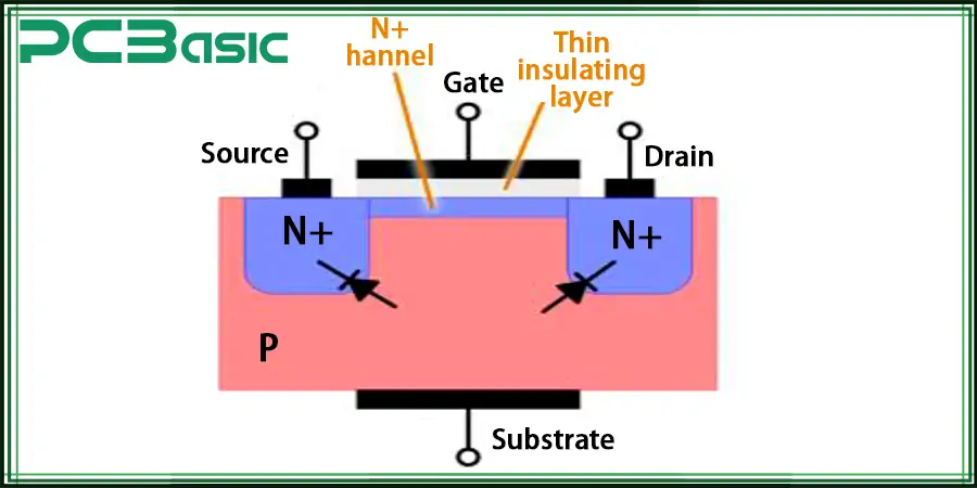
In our example, an NMOS transistor is fabricated on a p-type substrate with two n-type doped regions serving as the source and drain. A gate made of polysilicon or metal is placed over the channel region and is separated from the substrate by a very thin insulating layer of silicon dioxide (SiO₂). The gate controls the conductivity of the transistor by establishing an electric field that affects the transport of carriers in the channel.
1. Substrate & Doping
· Substrate: P-type (positively doped).
· Source & Drain: N-type (dopants are negative).
When there is no voltage applied to the gate, it will stay in an OFF state, and there will be no conductive path between the source and drain. But if the gate terminal is supplied with a positive voltage, then electrons from the source and drain regions are attracted to the channel. This creates an n-type inversion layer, allowing current to flow from the drain to the source. Current is a function of the gate-to-source voltage VGS and the drain-to-source voltage VDS.
2. Carrier Charge and the Current Flow
· Carrier: Electrons (high mobility)
· Active Mode: Drain to source in the ON state.
3. 'Gate Control' Outputs & Input Frame Voltage
· Turns ON when: Gate voltage is positive with respect to the source (VGS > Vth)
· Threshold Voltage (Vth): Lower than PMOS.
NMOS has electrons as charge carriers, which have higher mobility than holes (used by PMOS transistors). The higher mobility of electrons allows for quicker switching speeds, making NMOS transistors ideal for high-speed digital circuits. However, NMOS transistors also suffer from static power consumption because they also leak current when OFF.
4. Performance & Efficiency
· Switching Speed: Quicker due to electron mobility.
· Resistance: Low, leading to better efficiency and lower power loss.
5. Placement in CMOS Circuits
· Used in: Pull-down network (tie to ground).
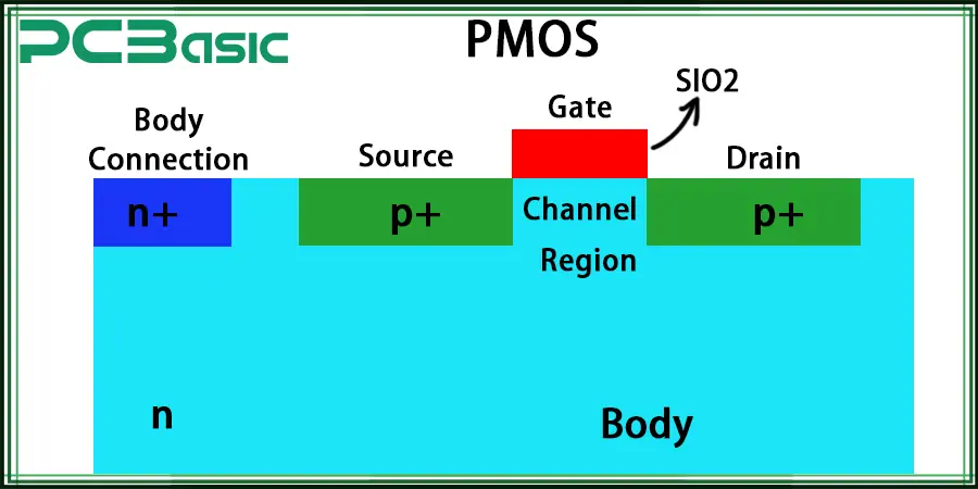
PMOS transistors consist of an n-type substrate with two p-type doped regions as source and drain. As an example, similar to NMOS, the gate rests on the channel separated by a thin layer of SiO₂, however, it operates differently due to holes being the charge carriers.
Because a hole has less mobility than an electron, PMOS transistors are always slower than NMOS transistors. This leads to longer switching delays so PMOS is less favorable in high-speed applications. Yet, PMOS transistors have superior characteristics in the OFF state, as it has less power in the OFF state which is an important point in low-power applications like battery-powered devices. About the aforementioned, PMOS transistors can be used in digital logic designs as pull-ups, ensuring that circuit nodes are at a high when they ought to be.
1. Substrate & Doping
· Substrate: n-type (negatively doped).
· Substrate: P type (positively doped).
In the absence of gate voltage, the transistor remains in an OFF state with no conductive channel. But when a negative voltage is applied to the gate it repels electrons from the channel region, creating a p-type inversion layer. This enables holes to migrate from the source to the drain, allowing for current flow. The PMOS transistor will remain ON as long as the gate voltage is lower than the source voltage with respect to the threshold voltage (Vth).
2. Charge Carriers & Current Flow
· Carrier Transport: Holes (low mobility)
· Working Direction: From source to drain we turn ON
3. Gate Controls & Threshold Voltage
· Turns ON when: Gate voltage is negative than source (VGS} < Vth).
· Threshold Voltage (Vth): Larger than the NMOS.
4. Performance & Efficiency
· Polarization Switching Speed: Slow as dictated by hole mobility
· Resistance: Greater, resulting in more power being dissipated.
5. Placement in CMOS Circuits
· Used In: Pull-up net (connect to Vdd)
NMOS and PMOS transistors can be modeled as Metal-Oxide-Semiconductor Field-Effect Transistor (MOSFET). In either case, their behavior is controlled by the voltage at the Gate (G) terminal, whether that causes a current to flow between the Source (S) and Drain (D) terminals.
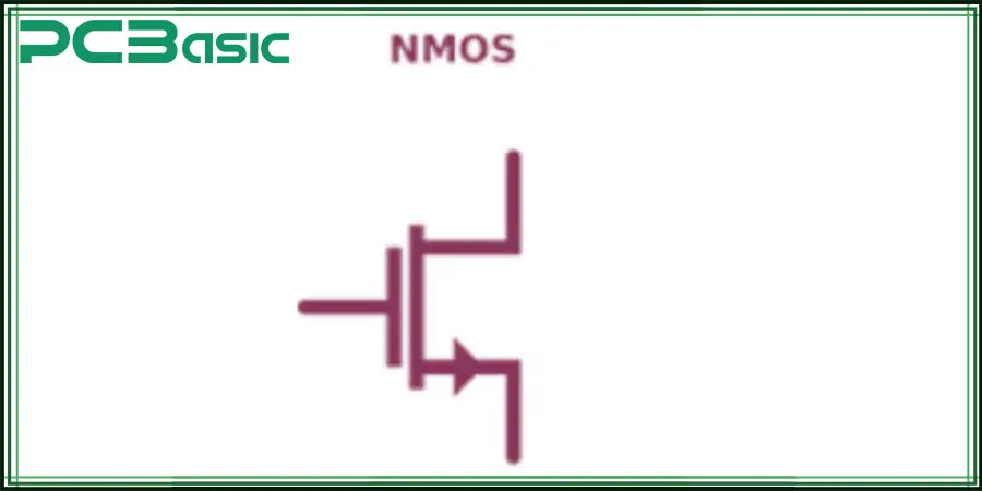
1. Structure & Charge Carriers
· The NMOS transistor represents a P-type substrate with an N-type Source and Drain regions.
· The majority of charge carriers are electrons.
2. ON State (Active Mode)
· When VGS is negative with respect to the source and is larger than the Threshold Voltage (Vth), electron get attracted between the Source and Drain, in what is called an "inversion layer".
· This forms a conductive channel that allows current to flow from the Drain to the Source.
3. OFF State
· No conductive channel is formed when VGS < Vth.
· The transistor stays OFF and does not allow current to flow.
4. Current Flow Direction
· Drain to Source when the transistor is ON.
5. Key Behavior
· Fast switching due to high electron mobility.
· Lower resistance and more efficient than PMOS.

1. Structure & Charge Carriers
· The substrate is N-type and the Source and Drain of the PMOS transistor is P-type.
· Majority charge carriers are holes.
2. ON State (Active Mode)
· VGS For negative gate voltage concerning the source, an inversion layer of holes is formed between the source and the drain.
· This forms a conducting channel, enabling current to pass the Source to the Drain.
3. OFF State
· Where VGS > Vth (Gate voltage is high or 0V), a conductive channel does not form.
· When the transistor is still OFF, no current will flow.
4. Current Flow Direction
· When the transistor is ON, there is a connection from Source to Drain.
5. Key Behavior
· Low hole mobility, which results in slower switching
· Greater resistance than NMOS, which causes more power loss
|
FEATURES |
NMOS (N-CHANNEL) |
PMOS (P-CHANNEL) |
|
Charge Carrier |
Electrons (high mobility) |
Holes (low mobility) |
|
ON Condition |
VGS > Vth |
Vth > VGS |
|
OFF Condition |
Vth > VGS |
VGS > Vth |
|
Current Flow Direction |
Drain to Source |
Source to Drain |
|
Switching Speed |
Faster |
Slower |
|
Resistance |
Lower |
Higher |
These transistors share different applications according to their conductive properties. They are commonly implemented in switching and amplification circuits.
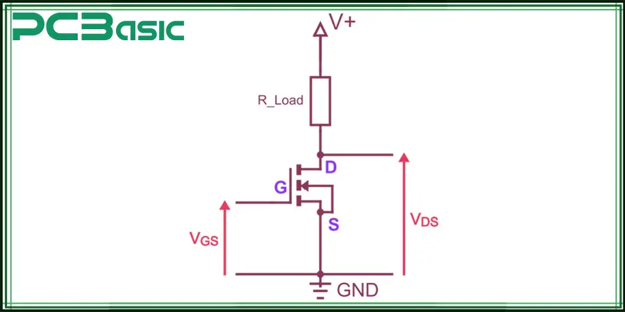
NMOS as a Switch
· The usual configuration for NMOS transistors is a low-side switch (ground).
· If the Gate voltage is high (VGS > Vth), the NMOS switch is ON, and current flows through the channel from Drain to Source.
· When the NMOS is OFF (Vth > VGS), current flow blocks.
Advantages:
· High electron mobility, which leads to faster switching.
· Reduced ON resistance for enhanced efficiency.
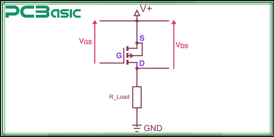
PMOS as a Switch
· PMOS transistors are used in high-side switching (connected to the power supply).
· PMOS turns OFF when VGS is greater than Vth.
Advantages:
· Used for power-switching in devices that run on batteries.
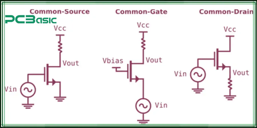
NMOS as an Amplifier
· Common-source amplifiers for voltage gain.
· Operates by varying the drain current through small changes in the gate voltage.
Advantages:
· RF and high-frequency applications, as it achieves high gain and high speed.
· Less distortion that either enhances or degrades signal quality.
PMOS as an Amplifier
· This is for analog circuits but is less common than NMOS amplifiers.
Advantages:
· Fixed performance in low-frequency analog circuits.
· Employed as low-power amplifier design.
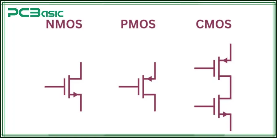
CMOS (Complementary Metal-Oxide-Semiconductor) technology is a prevalent semiconductor technology used in the design of digital circuits. It is a combination of NMOS (N-channel MOSFETs) and PMOS (P-channel MOSFETs) responsible for achieving low power consumption, high speed, and improved efficiency. Over the years, CMOS technology has become the basis of modern microprocessors, memory chips, and logic circuits, and plays a vital role in nearly all electronic devices in the world today.
The key advantage of CMOS in comparison to most CMOS single NMOS or PMOS logic is low power dissipation. CMOS only has substantial power during switching device, unlike NMOS logic which has static power due to a pull-down resistor. This property makes CMOS very suitable for battery driven devices and for large integrated circuits (LSI).
1. Structure of CMOS
· CMOS circuits are combinations of NMOS and PMOS transistors.
· NMOS transistors work as a pull-down switch (output gets connected to ground when active)
· The PMOS transistor is a form of pull-up switch (active connects output to Vdd)
· This pair acts complementarily minimizing power dissipation, since only one transistor is going to be working.
2. Working of CMOS Logic Gates
The simplest example is a CMOS inverter (NOT gate):
· When input is HIGH (1) → NMOS ON, PMOS OFF → Output will be LOW (0)
· If the input is LOW (0) then PMOS becomes ON, NMOS becomes OFF, and the output becomes HIGH (1).
For digital logic circuits (AND, OR, XOR, NAND, NOR gates), this means that CMOS is an ideal gate.
3. Advantages of CMOS
· Less Power Consumption: CMOS only consumes power on transition, whereas NMOS or PMOS has current flowing continuously..
· Less Influenced by Noise: CMOS circuits are indeed less influenced by system noise, keeping them stable.
· Quick switching speed: The realized speed in CMOS is higher than in PMOS since NMOS has low resistance.
· Scalability: CMOS technology scales well with transistor size which has made it the building block of modern semiconductor fabrication.
|
FEATURE |
CMOS |
NMOS |
PMOS |
|
Transistor Type |
Uses both NMOS and PMOS. |
Only NMOS. |
Only PMOS.
|
|
Power Consumption |
Very low. |
High. |
High. |
|
Switching Speed |
Fastest (optimized design). |
Fast. |
Slow. |
|
Resistance |
Balanced. |
Lower. |
Higher. |
|
Complexity |
Higher (dual transistors). |
Lower. |
Lower. |
|
Applications |
Digital circuits (microprocessors, logic gates). |
High-speed circuits. |
Low-power circuits. |
Therefore, it is important to know the differences between NMOS and PMOS before designing efficient and effective electronic circuits. NMOS provides faster switching, and PMOS provides complementary logic in CMOS. Modern integrated circuits have both to consume low power and to have high performance.

Assembly Enquiry
Instant Quote
Phone contact

+86-755-27218592
In addition, we've prepared a Help Center. We recommend checking it before reaching out, as your question and its answer may already be clearly explained there.
Wechat Support

In addition, we've prepared a Help Center. We recommend checking it before reaching out, as your question and its answer may already be clearly explained there.
WhatsApp Support

In addition, we've prepared a Help Center. We recommend checking it before reaching out, as your question and its answer may already be clearly explained there.