Global high-mix volume high-speed PCBA manufacturer
9:00 -18:00, Mon. - Fri. (GMT+8)
9:00 -12:00, Sat. (GMT+8)
(Except Chinese public holidays)
Global high-mix volume high-speed PCBA manufacturer
9:00 -18:00, Mon. - Fri. (GMT+8)
9:00 -12:00, Sat. (GMT+8)
(Except Chinese public holidays)
HomePage > Blog > Knowledge Base > Chip Scale Package (CSP)
As modern electronic products become smaller and more powerful, packaging technology is also improving. One important new technology is the chip scale package (CSP). This type of packaging is very small, but the performance is outstanding. Therefore, it is becoming more and more popular in the electronics industry.
This article will introduce you to what a CSP package is, its main features, the common types, such as WLCSP, LFCSP, FCCSP, and its advantages over traditional packaging methods.

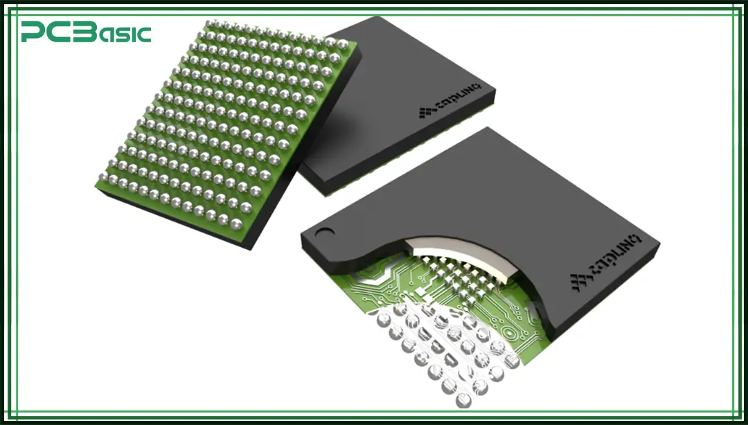
The Chip scale package (CSP) is an extremely compact packaging. It has a size almost as small as the chip itself. In other words, the chip no longer needs a large casing and takes up less space. Such a CSP package design not only allows more chips to be installed in a smaller space, but also brings better electrical performance. Among them, an important technological breakthrough is wafer level packaging. It completes the packaging process directly on the wafer without waiting for the chip to be cut down and then packaged. This way method can directly make the WLCSP package, which is the true sense of the chip scale package.
Unlike traditional packaging methods, CSP eliminates bulky lead frames and long wire bonds, instead utilizing advanced interconnection technologies for superior electrical performance and space savings.
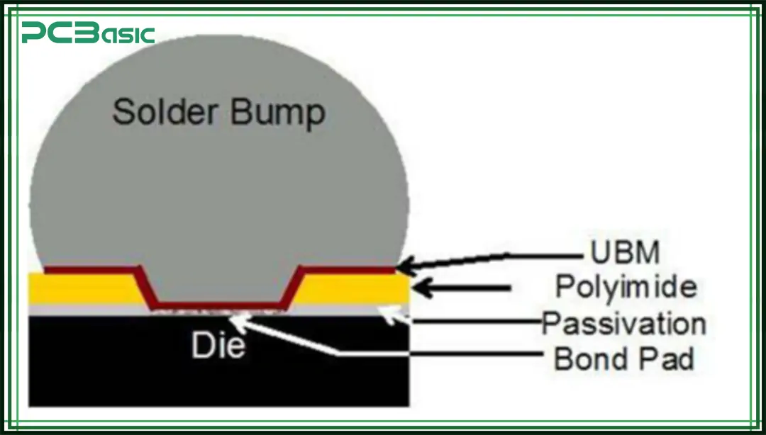
Key Components of CSP Construction
1. Die (Silicon Chip) – The core semiconductor device, typically thinned for ultra-low profile packaging.
2. Redistribution Layer (RDL) – A rewiring layer that routes I/O connections from the die pads to external terminals.
3. Solder Bumps/Pillars – Micro-scale conductive bumps (e.g., copper pillars or solder balls) for direct surface-mount attachment to PCBs.
4. Underfill/Encapsulation – Protective epoxy or molding compound that enhances mechanical stability and thermal performance.
5. Passivation Layer – A thin dielectric coating that safeguards the die from environmental and mechanical stress.

• Size Efficiency:
As the name suggests, a chip scale package is almost the same size as the chip itself, with little to no extra casing. This ultra-small packaging is especially suitable for space-constrained devices like smartphones, tablets, smartwatches, Bluetooth earphones, and other portable and wearable electronics.
• Improved Electrical Performance:
Because the internal connections of the chip are shorter, signal interference during transmission is reduced—things like inductance and resistance are minimized. This means signals travel faster and more stably, making it ideal for high-speed, high-performance applications.
• Cost-Effectiveness:
Especially when using wafer level packaging, many packaging steps can be done while the chip is still on the wafer, without waiting for it to be cut and processed later. This saves both materials and labor, reducing overall manufacturing costs, which is great for mass production.
• Thermal Performance:
The structure of the CSP package helps heat inside the chip transfer out more quickly, preventing overheating. So, even in high-load or high-performance situations, the system can still run reliably.
Among all types of CSP package, the most popular one is WLCSP. It completes all the packaging steps while still at the wafer stage, making it the smallest in size with very high reliability. Sometimes it's also called WCSP (Wafer Chip Scale Package) package, a name that highlights its wafer-level packaging nature.

Several common types of Chip scale packages have been developed according to different application requirements. Each type has its own unique structural design and application advantages. Here's a breakdown of the three main types:
|
Type |
Full Name |
Packaging Characteristics |
Performance Advantages |
Typical Applications |
|
WLCSP |
Wafer Level Chip Scale Package |
Packaged directly on the wafer; ultra-small size and thin profile. |
Saves space, high electrical performance, ideal for compact devices. |
Smartphones, IoT devices, wearables, camera modules. |
|
LFCSP |
Lead Frame Chip Scale Package |
Combines lead frame base with chip-scale design. |
Good heat dissipation, stable structure. |
Communication modules, power ICs, industrial control. |
|
FCCSP |
Flip Chip Chip Scale Package |
Uses flip chip bonding with solder bumps. |
High I/O density, strong thermal performance. |
High-speed processors, image chips, RF devices. |
While each CSP package type serves different engineering needs, WLCSP and its underlying wafer level packaging technology are undoubtedly at the core of today’s trend toward electronic miniaturization.
As semiconductor technology advances, packaging solutions have evolved to meet increasing demands for performance, power efficiency, and miniaturization. Chip Scale Packaging (CSP) has emerged as a popular alternative to traditional packaging methods, offering distinct advantages in many applications. Below, we compare these two packaging approaches across several key parameters.
Key Differences Between CSP and Traditional Packaging
|
Feature |
Chip Scale Packaging (CSP) |
Traditional Packaging |
|
Size |
≤1.2× the die size |
Typically 2-5× larger than die |
|
Weight |
Extremely lightweight |
Relatively heavier |
|
Profile |
Ultra-thin (<1mm typical) |
Thicker (1-3mm typical) |
|
Electrical Performance |
Shorter interconnects, better high-frequency performance |
Longer leads, more parasitic effects |
|
Thermal Management |
More challenging due to small size |
Generally better heat dissipation |
|
Cost |
Lower material cost, but may require more precise assembly |
Higher material cost, simpler assembly |
|
Reliability |
Excellent for small form factors |
Proven reliability for many applications |
|
Applications |
Mobile devices, wearables, IoT |
Automotive, industrial, legacy systems |
CSP represents a significant advancement in packaging technology, particularly suited for space-constrained applications where size, weight, and electrical performance are critical. The table shows how CSP packages are typically no more than 20% larger than the silicon die itself, compared to traditional packages that can be several times the die size.
However, traditional packaging still maintains advantages in certain scenarios. The larger form factor allows for better thermal dissipation and often simplifies board assembly processes. Many industrial and automotive applications continue to rely on traditional packaging solutions where extreme environmental robustness is required.
The choice between CSP and traditional packaging ultimately depends on the specific requirements of the application, with CSP dominating in consumer electronics and traditional methods maintaining strong positions in more demanding environments.
CSP packaging represents a major breakthrough in the semiconductor industry, simultaneously achieving three key advantages: compact size, high performance, and low cost. Common CSP variants like WLCSP, LFCSP, and FCCSP are now widely used in various electronic products including smartphones and smartwatches.
In simple terms, CSP technology enables smaller and more efficient chip packaging—exactly what modern smart devices need to keep evolving.

Assembly Enquiry
Instant Quote
Phone contact

+86-755-27218592
In addition, we've prepared a Help Center. We recommend checking it before reaching out, as your question and its answer may already be clearly explained there.
Wechat Support

In addition, we've prepared a Help Center. We recommend checking it before reaching out, as your question and its answer may already be clearly explained there.
WhatsApp Support

In addition, we've prepared a Help Center. We recommend checking it before reaching out, as your question and its answer may already be clearly explained there.