Global high-mix volume high-speed PCBA manufacturer
9:00 -18:00, Mon. - Fri. (GMT+8)
9:00 -12:00, Sat. (GMT+8)
(Except Chinese public holidays)
Global high-mix volume high-speed PCBA manufacturer
9:00 -18:00, Mon. - Fri. (GMT+8)
9:00 -12:00, Sat. (GMT+8)
(Except Chinese public holidays)
HomePage > Blog > Knowledge Base > Stripline in PCB Design: A Complete Guide
High-speed circuits need clean signals. No distortion and no interference. That’s why PCB designers use striplines. A stripline is a type of transmission line embedded between PCB layers. It keeps signals isolated and protected from external noise. That’s a big deal in RF, microwave, and high-frequency digital circuits.
But how does it work? Why choose it over a microstrip? And what should you know before designing one? Let’s find out in this blog.

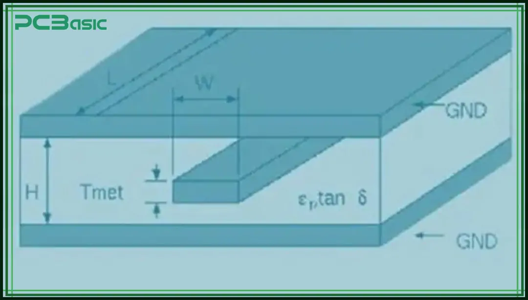
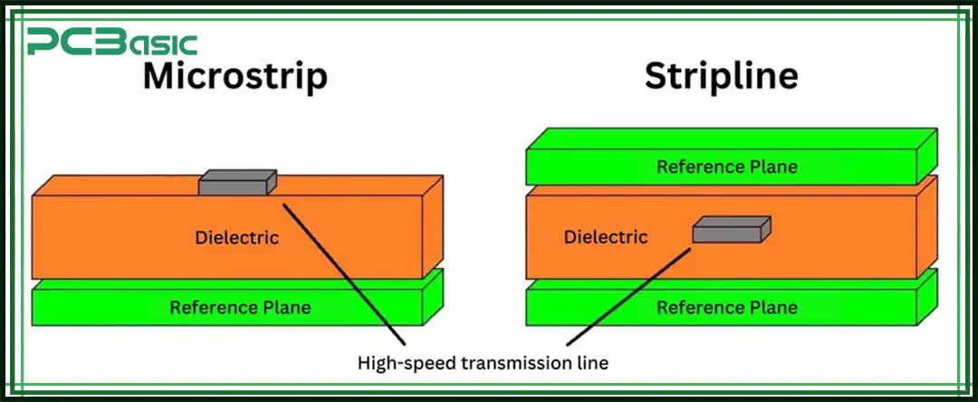
A stripline is a conductor placed between two ground planes inside a PCB. It’s completely buried within the board-- unlike microstrips, which are placed on the outer surface.
This design makes striplines electromagnetically shielded. Signals travel with minimal interference. Consequently, less crosstalk and more consistency.
Here’s a simple way to understand it:
• A microstrip is like a road—open and exposed to everything.
• A stripline is like a subway—protected, isolated from the outside world.
Striplines are commonly used in:
• High-speed PCBs for better signal integrity.
• RF and microwave circuits.
• Aerospace and defense electronics.
• Multi-layer PCBs with dense routing.

So, why go for a stripline instead of a microstrip?
Striplines sit between two ground planes. This acts like a shield, blocking interference from outside signals.
In high-speed designs, signals can degrade without hassle. Striplines offer a consistent impedance that reduces distortion.
Since striplines are buried inside the PCB, they don’t radiate as much energy as microstrips. That means fewer losses.
In dense PCBs, routing signals on the surface can be tricky. Striplines help by utilizing inner layers and keep the board layout clean.
However, there are trade-offs. Striplines are not easy to manufacture. They require precise layer stacking and dielectric control. They also have higher losses due to the surrounding dielectric material.
That’s why they are not always the best choice. It depends on the design.
When designing with striplines, a few things need your attention. Let’s break them down.
1. Material Choice: The material that surrounds the stripline is crucial. It’s called the dielectric material. Different materials have different properties, such as the dielectric constant. This affects how fast the signal travels through the line. You’ll need to choose a material that matches your specific needs for speed and signal quality.
2. Trace Width: The width of the copper trace in the stripline determines how much resistance it has. A wider trace means less resistance, which can help maintain the strength of the signal. On the other hand, a narrower trace increases the impedance. Balancing the trace width is key to getting the right impedance for your circuit.
3. Dielectric Thickness: The thickness of the dielectric material between the trace and the reference plane matters, too. Thicker dielectrics can slow down the signal, while thinner dielectrics speed it up. Finding the right balance is important for optimizing both signal speed and integrity.
4. Layering: The stripline is fully enclosed. Therefore, more layers are required in the PCB. This adds complexity to the design but provides better performance, especially in high-frequency applications. More layers mean more work in terms of manufacturing, but it’s often worth it for the benefits.
Striplines have their advantages, but they require careful planning. The materials, trace width, and thickness all play important roles in how the stripline behaves. Once you get these details right, your design will perform much better, reducing noise and ensuring the signal travels cleanly.

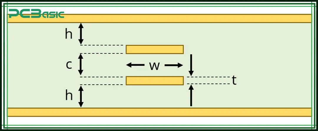
Getting the impedance right is critical in PCB design. If it’s off, signals can reflect and cause problems. Striplines follow a specific formula for impedance calculation. Here’s a simplified version:
Where:
• Z0 is the characteristic impedance (measured in ohms).
• εr is the dielectric constant of the material.
• h is the distance between the trace and the ground plane.
• w is the trace width.
• t is the trace thickness.
This formula helps engineers design circuits with the right impedance. Matching impedances reduces signal loss and improves reliability. If this seems complicated, don’t worry. Many PCB design tools have a built-in stripline impedance calculator to handle the math for you.
If manual calculations are not your thing, don’t worry. Many online tools can do the math for you. Here’s how they work:
1. Enter the material properties. Most calculators ask for the dielectric constant (εr) and layer thickness.
2. Input the trace width and thickness. These values affect impedance directly.
3. Set the spacing between layers—the distance between the trace and reference plane matters.
4. Click calculate. The tool will give you the exact impedance value.
Using a stripline impedance calculator saves time. It also reduces errors. Many PCB design software programs include built-in calculators for this purpose.
People often compare stripline vs. microstrip because they serve similar functions. But they have key differences.

1. Placement
• Striplines are buried inside the PCB, surrounded by dielectric material.
• Microstrips sit on the surface of the PCB and are exposed on one side.
2. Shielding
• Striplines are fully enclosed. This protects signals from external noise.
• Microstrips are more vulnerable to interference since one side is exposed.
3. Impedance Control
• Striplines provide a more stable impedance. This helps in high-speed circuits.
• Microstrips can be affected by external factors, making impedance harder to control.
4. Manufacturing Cost
• Striplines require more PCB layers. This increases cost and complexity.
• Microstrips are simpler and cheaper to produce.
So, which one is better? It depends. A PCB stripline is ideal for high-speed and low-noise applications. Microstrips work well for simpler designs that don’t need as much shielding.
Striplines are essential in modern PCB design. They provide excellent signal integrity, impedance control, and noise protection. Unlike microstrips, they are fully enclosed, reducing interference. However, they require more layers and precise calculations.
When designing with stripline, remember to choose the right dielectric material. Adjust trace width and thickness carefully. Plus, use an impedance calculator to get accurate values.
Striplines may take extra effort, but they improve performance. If your project involves high-speed signals, they’re worth considering. Want a hassle-free approach? Many PCB design tools simplify the process. Use them to optimize your PCB stripline layout and get the best results.

Assembly Enquiry
Instant Quote
Phone contact

+86-755-27218592
In addition, we've prepared a Help Center. We recommend checking it before reaching out, as your question and its answer may already be clearly explained there.
Wechat Support

In addition, we've prepared a Help Center. We recommend checking it before reaching out, as your question and its answer may already be clearly explained there.
WhatsApp Support

In addition, we've prepared a Help Center. We recommend checking it before reaching out, as your question and its answer may already be clearly explained there.