Global high-mix volume high-speed PCBA manufacturer
9:00 -18:00, Mon. - Fri. (GMT+8)
9:00 -12:00, Sat. (GMT+8)
(Except Chinese public holidays)
Global high-mix volume high-speed PCBA manufacturer
9:00 -18:00, Mon. - Fri. (GMT+8)
9:00 -12:00, Sat. (GMT+8)
(Except Chinese public holidays)
HomePage > Blog > Knowledge Base > How is Solder Mask Applied to PCBs?
A solder mask is a coating used to protect unused areas of copper traces on a printed circuit board (PCB) from solder attaching to them during the soldering process. Without this layer, solder can flow to places it shouldn't be, creating short circuits and making the device less reliable. This coating holds the solder where it should be during assembly, which also increases the life of the board.
In addition to preventing solder bridges, it also insulates the pads and their contacts from oxidation. It protects the board from moisture, dust, and other contaminants, such as liquid photo imageable (LPI) and dry film epoxy types.
Today, in our blog, we will take you through the solder masks, where they are used in PCB designing, and some points regarding the selection of solder masks, like thickness, expansion, and materials used.

A solder mask is a thin polymer layer on the PCB surface. Its primary intention is to inhibit unwanted soldering of copper traces when components are mounted. It also safeguards the board from humidity, oxidation, and dust that will ultimately impair performance.
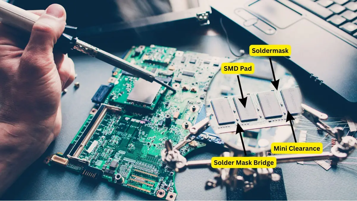
The solder mask layer is placed on top of the copper traces, and only the contact points are exposed. The solder mask openings, or solder mask holes, enable precise soldering of components. The mask color is green, but red, blue, black, and white may also be used depending on design and manufacturing requirements.
The proper solder mask enhances the reliability of the PCB with minimal opportunity for solder defects and electrical failure.
A solder mask consists of materials that insulate and protect copper lines on a PCB. These materials need to be able to handle high temperatures, be resistant to chemicals used in manufacturing, and be durable over time. The most widely used types are epoxy, liquid photoimageable (LPI), and dry film.
● Solder mask materials used
● Common solder mask materials
● Epoxy-based solder mask
● One of the most cost-effective options.
● Applied in liquid form and then hardened to create a solid protective layer.
● Offers sufficient insulation but is less precise than others.
● Most widely used in contemporary PCB manufacturing.
● Applied in liquid form, then exposed to ultraviolet light with a mask applied to create holes.
● Offers high precision, suitable for fine-pitch components.
● Sold in pre-manufactured sheets laminated to the PCB.
● Offers high coverage and precision but is less utilized than LPI.
● Used in specialist applications where high precision is required.
Solder masks must withstand harsh environments during wave soldering and reflow processes. The materials utilized are formulated to:
● Withstand high temperatures without degrading.
● Resist flux, solvents, and cleaning chemicals used to assemble the PCB.
● Withstand electrical insulation under harsh conditions.
The choice of solder mask material depends on the PCB application, manufacturing, and durability level.

Solder mask application onto a PCB requires a few steps to deposit the appropriate amount and cover the appropriate areas. The process needs to be accurate to provide the appropriate electrical insulation with uniform solder contacts.
The surface of the PCB needs to be cleaned prior to solder mask application. Adhesion problems are due to dust, oil, or oxidation. The process typically involves:
● Chemical cleaning to remove residues.
● Brushing and rinsing to smooth the surface.
● Drying to prevent moisture-based defects.
The solder mask material selected—epoxy, liquid photo imageable (LPI), or dry film—is applied by one of the following methods:
● Screen printing for epoxy-based masks.
● Spraying or curtain coating for LPI masks.
● Vacuum lamination for dry film masks.
● The application must be even to prevent weak spots or excessive buildup.
After application of the solder mask, it must be shaped into the PCB design:
● UV light exposure – A mask of the PCB design is placed over the board, and UV light hardens the areas to be left intact.
● Developing – Exposed areas are washed away, leaving precise openings for soldering.
For the solder mask to be hardened, the PCB is cured—usually in an oven or UV light. This hardens the material, resisting heat, chemical and mechanical stress damage.
The solder mask openings should be accurately aligned with component pads in order to facilitate proper soldering. An opening that is too big will result in solder bridges. An opening that is too small will result in incomplete soldering.
A properly applied solder mask enhances the reliability of the PCB as well as makes the assembly easy.
The solder mask selection varies with the manufacturing process, durability requirements, and environmental conditions. All types offer various benefits that are dependent on the application.
● Application: Screen printing
● Durability: Fair resistance to heat and chemicals
● Best For: Economical, high-rate methods
● Liquid photoimageable (LPI) Solder Mask
● Tech info: Spray- or curtain-coating, followed by UV exposure
● Durability: Greater precision, stronger adhesion
● Ideal for: Fine-pitch components, multilayer boards
● Devise: Vacuum lamination, UV exposure thereafter
● Durability: Even thickness, best for regulated designs
● Most suitable for High-density circuits, complex PCB designs
● Green: Standard, highest contrast for checking
● Transparent: Simplified internal trace inspection
● Low-Cost and High-Volume Production: Ideal for Epoxy-based masks
● LPI or dry film: High Precision or High-Density Circuits
● For Harsh Environments: Select high chemical and heat resistance material.
● For Aesthetic or Branding Needs: Custom colors and transparent backgrounds
Using the appropriate solder mask promotes reliability and simplifies assembly.

An adequate solder mask design can benefit PCB robustness, soldering accuracy and electrical performance. The mask will protect traces and devices to some degree, depending on how well.
Solder mask expansion – How much the mask gobs over a pad/tracer. Too big an expansion can potentially expose more areas than necessary, which is prone to oxidation.
● Keep the pads from touching any other pads to avoid wrong connections.
● Follow manufacturer guidelines to avoid potential mask adhesion problems.
● Automated design tools are useful to make sure they are aligned correctly.
Correct thickness stops short circuits, oxidation, and solder wetting. Typical standard values varied from 0.7 mil to 1.5 mil depending on PCB type.
Impact of thin layers on performance:
We improve the accuracy for fine-pitch components, but they might wear out faster as well. Thicker Layers provide higher insulation potential, risking uneven soldering
● High-voltage: Need thicker masks for electrical load.
Material selection has an influence on heat resistance, chemical stability and durability. Specifically, they can be:
● Epoxy: Cheap, not durable.
● Liquid Photoimageable (LPI): Gives you more accurate coverage, which is better for anything nice-looking.
● Dry film: makes it the same thickness and has sharp edges.
Solder mask openings are created where copper pads have to be soldered, and other unintended connections are forbidden.
● Be sure that it is properly located and does not mask the solder pads.
● Medium-perf circuit designs with Masked pads.
● So, one can further dissect this behavior by splitting the trace even more.
An excellent solder mask helps improve defects, makes you able to put together your PCB that is easier and prolongs the Level of Life.
The vast majority of the various functionalities of both the mask plating and etch mask functions are your printed circuit board machinist. They are not used separately, but it has some other features other than other types of soldering levels.
|
Feature |
Solder Mask |
Paste Mask |
|
Purpose |
Prevents copper traces from oxidizing and short circuits |
Regulates solder paste application for component placement |
|
Material |
Epoxy, Liquid photoimageable (LPI), or dry film |
Stencil openings were applied to place solder paste |
|
Application |
Applied to the entire PCB with pads exposed |
Applied to a stencil that is aligned with component pads |
|
Effect on Soldering |
Prevents solder bridging and dirt contamination |
Guarantees proper solder is deposited on pads |
Literally, all PCB strength and accuracy of production derive from the solder mask. It also prevents oxidation of copper traces, provides solder with a fighting chance of not bridging, and is an insulator that makes sure that the board will actually do the thing that it is supposed to do. Thickness, expansion and material selection stabilize component placement and soldering. Solder mask—utilized for long-term insulation and protection for a PCB Paste mask—printed during the SMT assembly process for solder paste. Knowing the differences and advantages of each provides greater performance and reliability in PCBs. A properly applied solder mask not only makes the assembly more efficient but also prolongs the life of the circuit board.

Assembly Enquiry
Instant Quote
Phone contact

+86-755-27218592
In addition, we've prepared a Help Center. We recommend checking it before reaching out, as your question and its answer may already be clearly explained there.
Wechat Support

In addition, we've prepared a Help Center. We recommend checking it before reaching out, as your question and its answer may already be clearly explained there.
WhatsApp Support

In addition, we've prepared a Help Center. We recommend checking it before reaching out, as your question and its answer may already be clearly explained there.