Global high-mix volume high-speed PCBA manufacturer
9:00 -18:00, Mon. - Fri. (GMT+8)
9:00 -12:00, Sat. (GMT+8)
(Except Chinese public holidays)
Global high-mix volume high-speed PCBA manufacturer
9:00 -18:00, Mon. - Fri. (GMT+8)
9:00 -12:00, Sat. (GMT+8)
(Except Chinese public holidays)
HomePage > Blog > Knowledge Base > High Voltage PCB Design: Clearance, Spacing & Arc Prevention Tips
Designing a high voltage PCB is not just about scaling up a standard PCB. It requires critical considerations in preventing arcing, ensuring safety and maintaining long-term performance.
This article will explore how to optimize high voltage PCB design for safety and reliability, from high voltage clearance distance, PCB track spacing to insulation, and more.

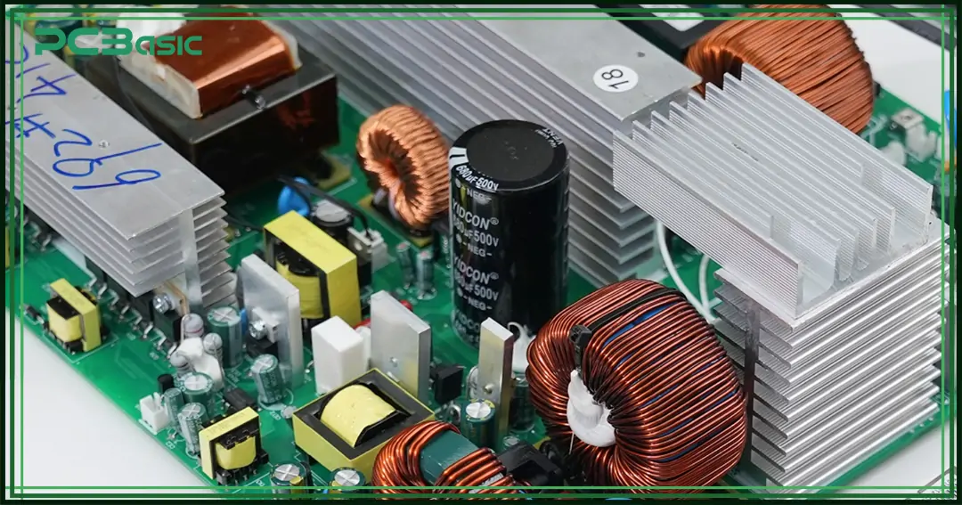
The high voltage PCB is a printed circuit board specially designed to withstand high voltage, which is usually suitable for applications where the voltage is much higher than that of standard circuit boards, such as voltages ranging from several hundred volts to several thousand volts.
Compared with regular PCBs for low voltage digital or analog signals, high voltage PCBs need to be designed with a focus on how to prevent electrical breakdown of insulation layers, how to avoid arcing through air, and how to ensure that there is sufficient clearance between conductive elements.
Therefore, in the high voltage PCB design, key considerations such as the selection of insulation materials, the setting of high voltage clearance distance, the reasonable arrangement of PCB trace spacing and implementing structural isolation methods are very important to ensure safety and reliability.

High voltage PCBs are commonly used in equipment that requires high voltage handling and operates in complex environments, such as:
• Power supplies and power converters:
These devices are used to convert voltage levels, such as from AC to DC or from low voltage to high voltage.
• Electric vehicle systems:
In electric vehicles, components like motor drives, battery management systems (BMS), and charging systems involve the transmission and control of high-voltage currents.
• Industrial automation equipment:
Equipment such as large machinery, robotic arms, inverters, and motor control systems often deal with high-power and high-voltage signals or loads.
• Medical devices (such as defibrillators):
Some medical devices need to deliver a sudden burst of high voltage—defibrillators, for example, can generate shock voltages in the thousands of volts.
• Aerospace and defense systems:
These systems operate in extreme environments, such as high altitudes, low pressure, and high humidity, requiring circuit boards with outstanding stability and safety.
In all of the above applications, without a reliable high voltage PCB design for arc prevention, it may result in circuit failure, arcing, or even personal injury. Therefore, the design stage must focus on insulation, spacing, materials and other factors to ensure the safe, stable and durable operation of the equipment under high pressure environment.
If you're designing a circuit board that needs to work in a high-voltage environment, you can't just draw it like a regular PCB. When the voltage is high, it's easy to get sparks, current leakage, or even burn out the circuit. So you need to be extra careful during the design process. The following areas must be given special attention:
These two terms sound technical, but they’re actually easy to understand:

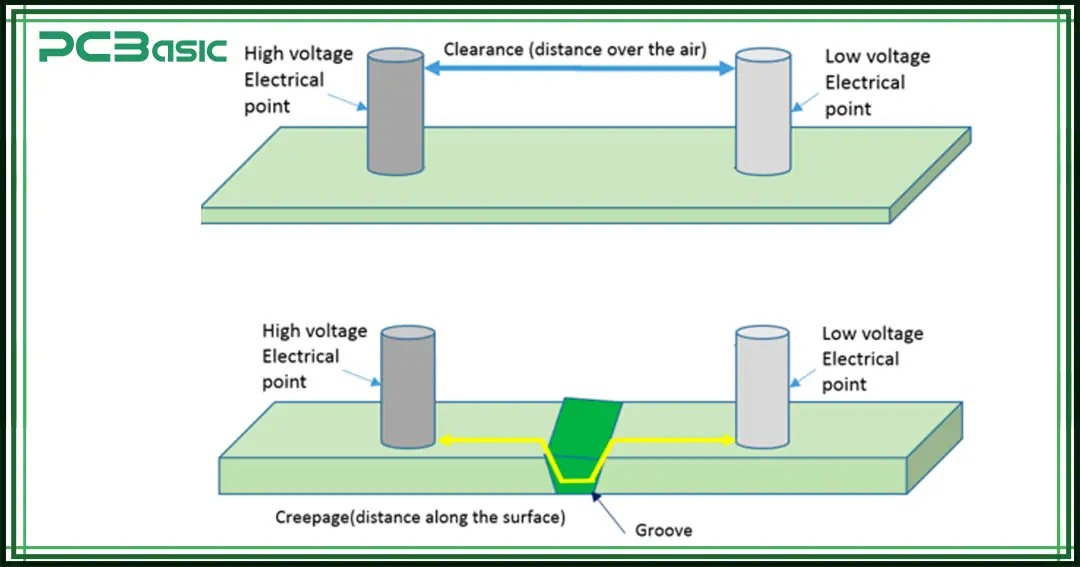
• Clearance: This is the shortest distance “through the air” between two live metal parts. If they’re too close, high voltage can break down the air and cause a spark (arc).
• Creepage: This is the shortest path current might “crawl along” the surface of the PCB. If the surface is dusty, moist, or dirty, it’s even more likely to leak electricity.
So when you design, make sure there’s enough distance between live parts. If they’re too close, the current might “jump through the air” or crawl across the board surface.
When the voltage gets high, you can't just use any material.
In simple terms: using the right material keeps the voltage from “breaking through.”
Besides keeping parts apart and choosing good materials, there are extra ways to improve insulation:
• Conformal coating: Spray a protective layer on the board surface to keep out moisture, dust, and corrosion.
• Potting or encapsulation: Fill the whole board or key areas with glue or resin so the current has nowhere to go.
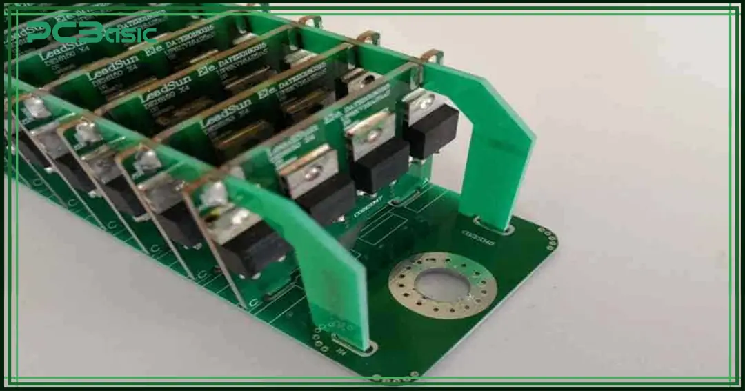
• Isolation slots: Cut grooves into the board to physically separate high-voltage areas from the rest, forcing the current to take a longer, safer path.
These tricks help “lock in” the voltage so it can’t leak out or jump around.

• Board thickness: The thicker the board, the better it can resist being broken down by high voltage.
• Trace spacing: The space between copper lines needs to be wide enough. If the traces are too close, high voltage might jump across them.
A common rule of thumb is: leave at least 2.5 mm of spacing for every 1000 volts. So for 3000 volts, you’d need at least 7.5 mm.
This might make your board bigger, but it’s worth it for safety.
• For the board surface, use a high-quality finish like ENIG (Electroless Nickel Immersion Gold). It prevents oxidation and improves conductivity, which is great for high-voltage boards.
• For the little holes on the board (called vias), don’t leave them exposed. Cover them or fill them so they don’t become paths for electrical arcs.
Designing a high-voltage PCB basically comes down to one simple idea:
Make the current follow the path it’s supposed to, and don’t let it jump, arc, or leak.
To do that, you need to choose the right materials, give parts enough space, apply proper insulation, use thicker boards, and pay attention to the details. If you handle all these key areas properly, your high-voltage PCB will be able to operate safely and reliably for a long time.
If you’re doing product design, handling procurement, or just starting out in the PCB industry, these are the most basic but essential safety principles you need to understand.

Assembly Enquiry
Instant Quote
Phone contact

+86-755-27218592
In addition, we've prepared a Help Center. We recommend checking it before reaching out, as your question and its answer may already be clearly explained there.
Wechat Support

In addition, we've prepared a Help Center. We recommend checking it before reaching out, as your question and its answer may already be clearly explained there.
WhatsApp Support

In addition, we've prepared a Help Center. We recommend checking it before reaching out, as your question and its answer may already be clearly explained there.