Global high-mix volume high-speed PCBA manufacturer
9:00 -18:00, Mon. - Fri. (GMT+8)
9:00 -12:00, Sat. (GMT+8)
(Except Chinese public holidays)
Global high-mix volume high-speed PCBA manufacturer
9:00 -18:00, Mon. - Fri. (GMT+8)
9:00 -12:00, Sat. (GMT+8)
(Except Chinese public holidays)
HomePage > Blog > Knowledge Base > What is a Gerber File?
Have you ever wondered how all the details on your PCB design get transferred to a tangible copper board? Read on to uncover the critical role of Gerber files in PCB fabrication!

(3D view of a PCB design awaiting fabrication in KiCad 3D Viewer)
As a PCB design engineer, the end effort you put into your design in terms of getting your design to pass the Design Rule Check (DRC), Electrical Rule Check (ERC), Signal Integrity Analysis (SI), and even the Design for Manufacturing (DFM) is to the end that you can get you circuit working flawlessly. However, for your design to be fabricated, there is a need for effective manufacturing instruction, which requires generating the proper Gerber file format for fabrication.
A Gerber file is to a finished Printed Circuit Board (PCB), which is what a script is to a play. Just as a script provides actors with lines, cues, and stage directions, a Gerber file gives the PCB manufacturing machines precise instructions for producing the exact design created by a PCB design engineer.
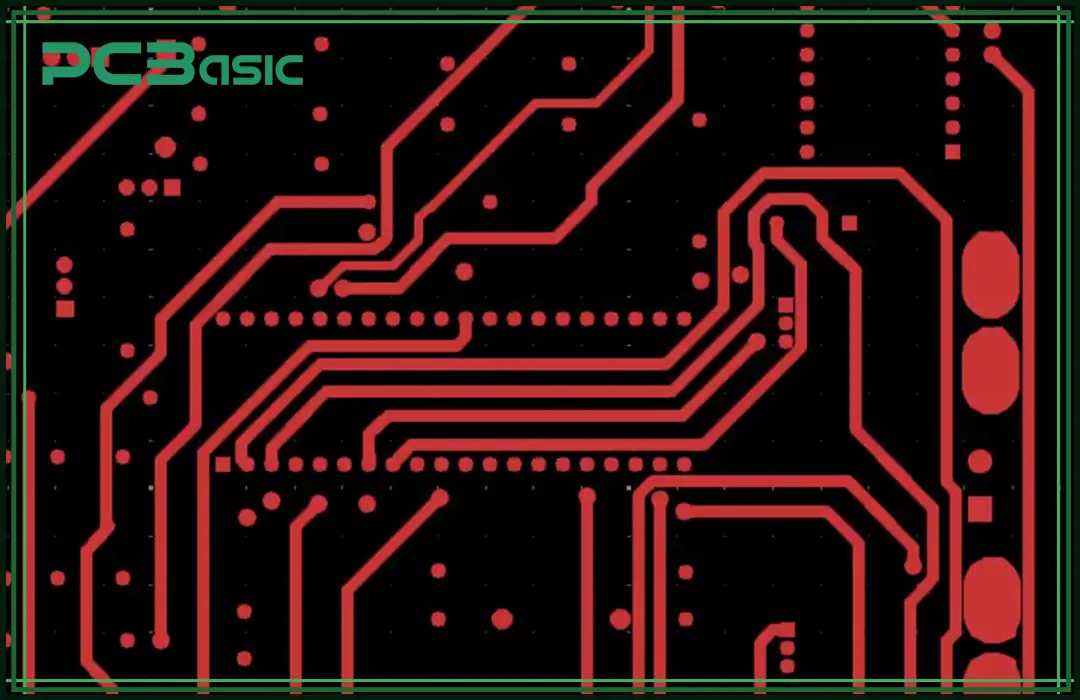
(Front Copper view of a PCB designed opened with a Gerber viewer)
Although the Gerber file is not the only output file used in PCB manufacturing, there are others like the ODB++ and IPC-2581 However, the to interpret it. Gerber file format remains the most popular. In this article, you will understand the Gerber file format, its unique role in PCB fabrication, and how to use a Gerber file viewer
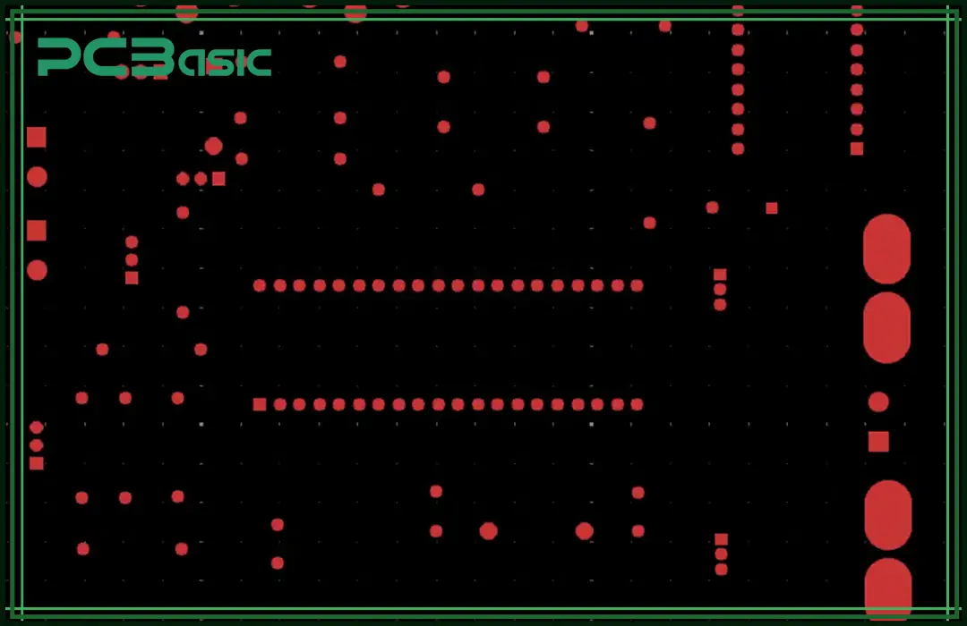
Gerber files primarily store all information on the PCB design layout in a form that can be interpreted by the Computer Aided Manufacturing software (CAM). The data in the Gerber file includes the XY coordinate for the draw and flash command, Aperture definition, and draw and flash command code—configuration parameter.
Simply put, the Gerber file is the transcript of a PCB design that can be easily understood by the fabrication machines. To view or edit these files, engineers use Gerber file viewers and Gerber file editors.
The Gerber file format was developed in the 1960s by Gerber Systems Corporation, a company founded by Joseph Gerber; at that time, several companies in the electronics industry were quickly adopting the idea of PCB layout for their electronics products, making the Gerber file format grow famous in the electronics world. From the first introduction of the Gerber file format first version till date, it has evolved significantly, with each update bringing greater sophistication, accuracy, and ease of data transfer designers to manufacturers.
The evolution of the Gerber Format includes:
1. RSD-274-D
2. RS-274X
3. Gerber X2 Format
4. ODB++
Overview of different Gerber Format
1. RSD-274-D: Gerber Systems Corporation created the RS-274-D Gerber file format in the 1960s basically to control photoplotters for generating films used in PCB production. This early format used the XY coordinate locations alongside draw and flash commands to define shapes. However, engineers had to manually assign aperture codes specifically for aperture definition during the file creation.
2. RS-274X: Later in the 1980s, the RS-274X Gerber file format was introduced to address many of the limitations of the earlier RS-274-D format. One significant improvement in the later version was its ability to handle aperture information within the same file directly. These remove the need for separate aperture definitions. Despite the improvement, the RS-274X Gerber format still requires the inclusion of multiple other files to represent different PCB layers and drill data.
3. Gerber X2 Format: The introduction of the Gerber X2 format is a significant breakthrough in the electronics industry. Although it is designed to be compatible with the existing RS-274X Gerber file viewers and Gerber software, it comes with extra attributes and features that make the design-to-manufacturing process seamless. The key features of the Gerber file include
• Layer stack definitions
• Drill data
• Component data such as part numbers, values, and footprints
• Impedance control
• Netlist data
Backward compatibility (This implies X2 maintains compatibility with existing RS-274X viewers and Gerber software)
4. ODB++: The ODB++ format embeds all necessary data for PCB production—including layer structures, drill data, material stack-up, netlist with test points, component bill of materials (BOM), component placement, and fabrication data—into a single archive.
|
Gerber Format Name |
Year Introduced |
Key Features |
Limitations |
Advancements |
|
RS-274-D |
1960s |
- Controls photoplotters for generating films used in PCB production. - Uses XY coordinate locations, draw, and flash commands to define shapes.- Aperture codes had to be manually assigned for aperture definition. |
- Aperture codes are manually assigned for aperture definition. |
- First standard for PCB production. |
|
RS-274X |
1980s |
- Handles aperture information within the same file, removing the need for separate aperture definitions. |
- Multiple files are still required to represent different PCB layers and drill data. |
- Addresses limitations of RS-274-D and reduces manual input errors. |
|
Gerber X2 |
2014 |
- Layer stack definitions. - Drill data. - Component data (part numbers, values, footprints). - Impedance control. - Netlist data. - Backward compatibility with RS-274X viewers and Gerber software. |
- Limited adoption in some areas. - Compatibility issues with older systems. |
- Seamless design-to-manufacturing process. - Improves automation and includes detailed design information. |
|
ODB++ |
1990s |
- Embeds all necessary data for PCB production into a single archive. - Includes layer structures, drill data, material stack-up, netlist with test points, component BOM, and component placement. |
- Larger file size. - Not as universally supported as Gerber formats. |
- Highly efficient - Reduces human error, not bad for modern PCB production |
Just like .mp3 files indicate audio files, different Gerber file extensions describe different layers and functions in a PCB design. Here are some common Gerber file types:
• APT: Aperture File
• APR: Aperture File
• DRL: Drill Data
• DRR: Drill Tool Size
• EXTREP: Extension Report of Gerber Files
• GBL: Gerber Bottom Layer
• GBS: Bottom Solder Mask
• GBP: Bottom Paste
• GBO: Bottom Overlay
• GPB: Pad Master Bottom
• G1, G2, etc.: Mid-layer 1, 2, etc.
• GD1, .GD2, etc.: Drill Drawing
• GG1, .GG2, etc.: Drill Guide
• GM1, .GM2, etc.: Mechanical Layer 1, 2, etc.
• GP1, .GP2, etc.: Internal Plane Layer 1, 2, etc.
• GKO: Keep Out Layer
• GTL: Gerber Top Layer
• GTP: Top Paste
• GPT: Pad Master Top
• GTO: Top Overlay
• GTS: Top Solder Mask
• LDP: Layer Pairs Export File for PCB
• P01,. P02, etc.: Gerber Panels
• REP: Report of Individual Layer Used Aperture List
• RUL: DRC (Design Rule Check) Rules
• TXT: Drill Position
Literarily, whenever a Gerber file is opened, you see a sequence of known characters, which include alphabets, numbers, and special characters. The question remains: what sort of data is represented by those ASCII data? A simple answer to this is that the encoded data seen actually holds critical information about each of the layers of the PCB layout. These layers include:
• Top Copper (Top Layer)
• Top Solder Mask
• Top Paste Layer
• Silkscreen
• Drill Data
• Board Outline
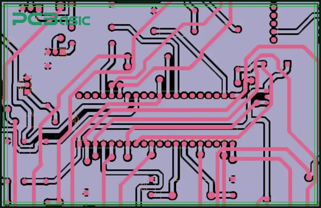
(Multiple layer view of a Gerber file)
As an engineer, you may need to open your Gerber file for several reasons. It could be for error checks, design analysis, or even information sharing with your team. With a suitable Gerber file viewer, opening a Gerber file is straightforward. As a matter of fact, many of the existing viewers also serve as Gerber file editors, allowing you to make adequate adjustments as needed. Here are some recommended Gerber viewers you can explore as an engineer:
· Gerbv
· KiCad
· Altium Designer
· OrCAD PCB Designer
· GerberViewer.org
· PCBWay Online Gerber Viewer
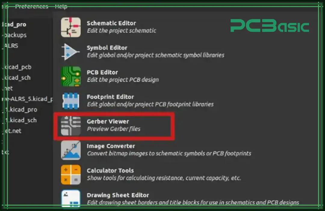
(Gerber viewer software in KiCad)
Here’s a practical application guide for creating and exporting Gerber files using Eagle, Altium Designer, and EasyEDA:
1. Eagle:
1. Open the PCB project in EAGLE.
2. Run the Design Rule Check (DRC) to ensure the layout passes all checks.
3. Go to the File menu and select CAM Processor.
4. Select the pre-configured CAM job or load a suitable one if needed.
5. Click the Process Job button to generate the output files.
6. Specify an output directory when prompted.
7. Review the final summary and click OK to confirm.
8. The Gerber files are generated in the defined output folder.
9. A job report is also created detailing the file outputs.
2. Altium Designer:
1. Open your PCB project in Altium Designer.
2. Navigate to file > Fabrication Outputs > Gerber Files.
3. In the Gerber Setup dialog, select the layers to plot by clicking Plot Layers and then Select Used.
4. Go to the Advanced tab, configure the settings as required, and click Apply.
5. Close the pop-up—Cam project window without saving.
6. Go to file > Fabrication Outputs > NC Drill Files
7. to generate the drill files.
8. Configure the drill settings in the NC Drill Setup dialog and click OK.
9. The Import Drill Data window will pop up, keep the default settings, and click OK.
10. The Gerber and drill files are now exported and available in the specified output folder.
3. EasyEDA:
1. Open your project in EasyEDA.
2. Click on Document and select Generate Fabrication File (Gerber).
3. If prompted, click No, Generate Gerber to proceed.
4. Click on Generate Gerber.
5. Save the file at your preferred location with a chosen file name.
6. The software will generate a .zip file containing all necessary Gerber files.
7. This .zip file can be uploaded to platforms such as Lion Circuits when placing an order.
Gerber file errors might occur for a variety of reasons. In most cases, the PCB is hindered from being fabricated seamlessly. Some of the possible errors you might encounter while trying to open a Gerber file include:
1. Missing Drill Files.
2. Outline Errors potentially resulting in incorrect board dimensions.
3. Mismatched PCB Size and Drill Hole.
4. Layer Labelling and component arrangement Errors.
5. Multiple Aperture Lists
Gerber and CAD files serve different purposes and differ in output formats and usage. Gerber files are standard outputs designed mainly for PCB manufacturing. The Gerber file contains detailed data for each board layer, including copper traces, drill holes, and solder masks. On the other hand, CAD files are used for PCB design, and they contain more comprehensive information, such as schematics, component placement, and electrical routing. CAD files are generally proprietary to the software used for designing alone. In contrast, Gerber files are universal and focused on conveying manufacturing instructions in a way that all fabrication tools can interpret.
When it comes to the generation process, CAD files are typically created by design software like Altium Designer, KiCad, or Eagle. These software are quite sophisticated, and they are capable of doing quite a number of other things, which include simulation, component management, and other features. Once the design process is complete, the CAD software usually exports Gerber files specifically for fabrication. Tools such as the CAM processor in Eagle or the Gerber file generator in Altium are commonly used for this purpose.
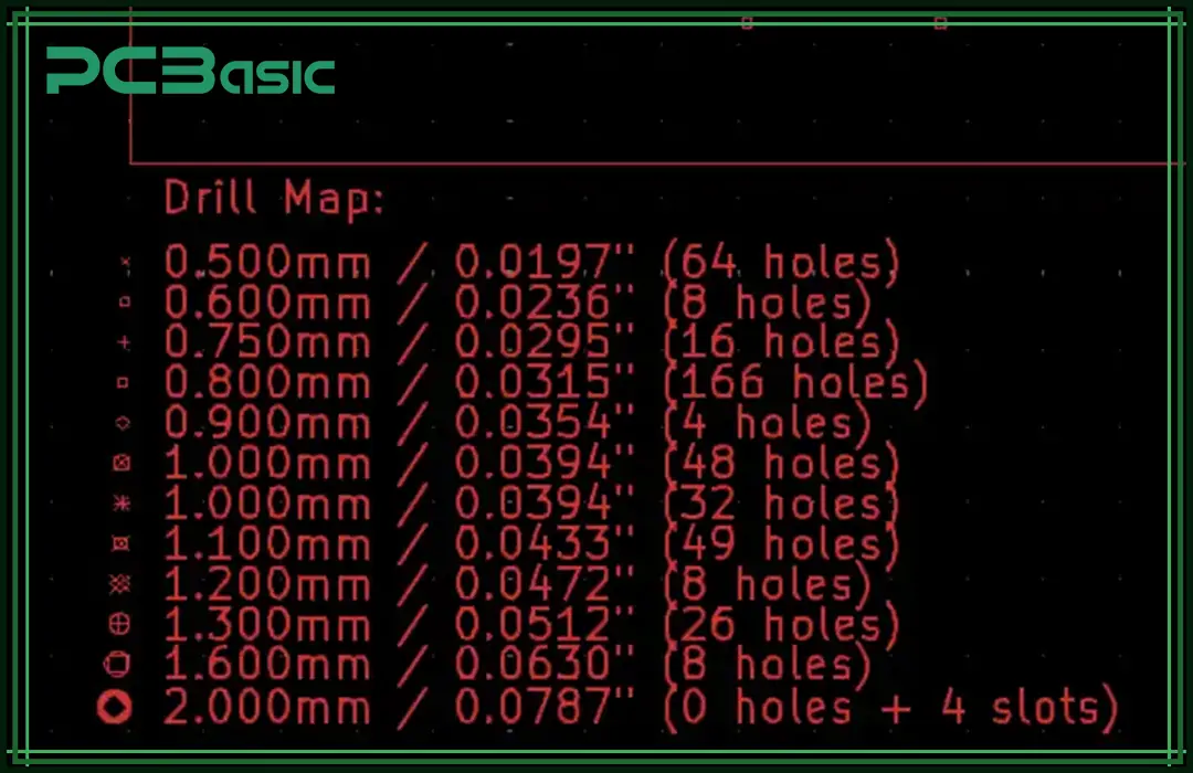
Every successfully designed PCB relies on a well-structured Gerber file containing all necessary Gerber data such as copper traces, drill data, and solder masks. The Gerber file format is the universal standard for PCB manufacturing, ensuring accuracy and reliability across the industry.
Understanding what is a Gerber file, knowing how to open Gerber files, and utilizing a Gerber file viewer or Gerber software are crucial steps for engineers. By following best practices, you can ensure that your Gerber files are flawless and ready for fabrication.

Assembly Enquiry
Instant Quote
Phone contact

+86-755-27218592
In addition, we've prepared a Help Center. We recommend checking it before reaching out, as your question and its answer may already be clearly explained there.
Wechat Support

In addition, we've prepared a Help Center. We recommend checking it before reaching out, as your question and its answer may already be clearly explained there.
WhatsApp Support

In addition, we've prepared a Help Center. We recommend checking it before reaching out, as your question and its answer may already be clearly explained there.