Global high-mix volume high-speed PCBA manufacturer
9:00 -18:00, Mon. - Fri. (GMT+8)
9:00 -12:00, Sat. (GMT+8)
(Except Chinese public holidays)
Global high-mix volume high-speed PCBA manufacturer
9:00 -18:00, Mon. - Fri. (GMT+8)
9:00 -12:00, Sat. (GMT+8)
(Except Chinese public holidays)
HomePage > Blog > Knowledge Base > Transistor Pinouts: The Ultimate Guide
Proper identification of transistor pins is an essential skill for anyone dealing with electronic circuits. Whether you are a hobbyist constructing your first amplifier or a seasoned engineer repairing intricate systems, knowing transistor pinouts avoids expensive errors and guarantees correct circuit function. Transistors usually have three connecting pins (legs), each with a different purpose. But their positioning is quite different among transistor families and even between models of the same type produced by different manufacturers. This is why a guide to transistor pinouts is necessary for electronics engineering.
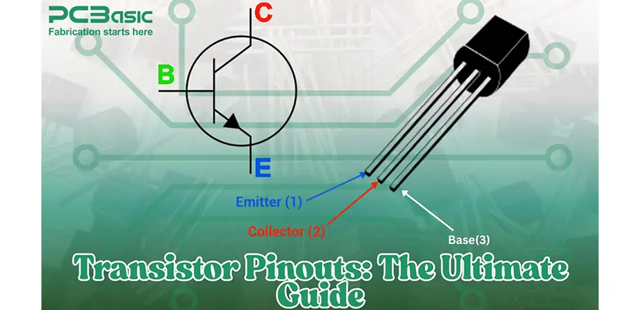
To determine transistor pins correctly, you'll require:
● The manufacturer's datasheet (most authoritative source)
● Information about the transistor package type
● Knowledge about manufacturer-specific codes for markings
● Knowledge about model-specific differences
As we continue with this guide, you'll learn what you need to know to identify confidently and properly apply different types of transistors in your electronic projects and prevent the aggravation of circuit failure due to improper pin identification.
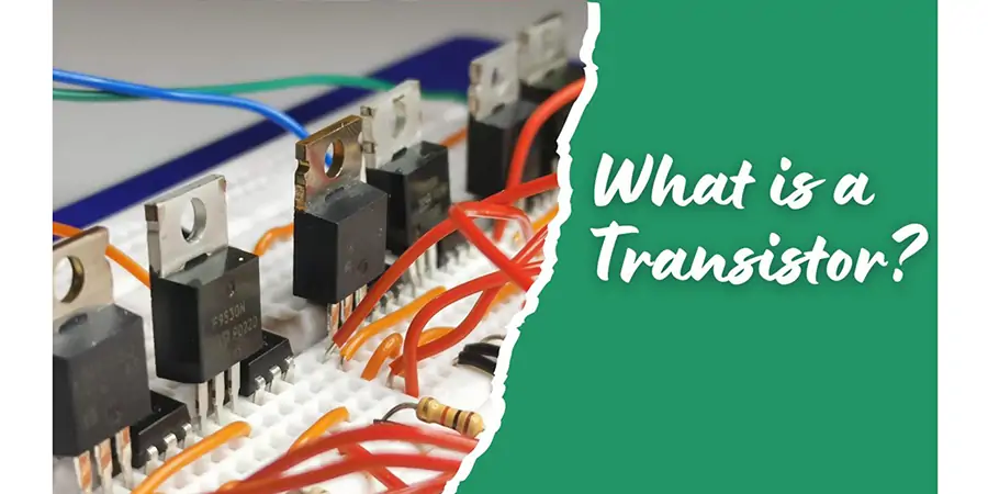
The transistor revolutionized electronics as one of the most important inventions in the 1900s. This small semiconductor device controls electric currents and acts as both amplifiers and switches in electronic circuits. Essentially, a transistor can increase weak signals or act as an electronic port, making it a basic building block in almost all modern electronic systems.
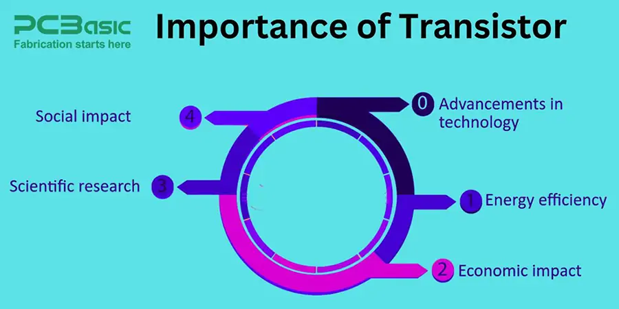
Mass production of transistors through automation has significantly reduced costs. As a result, transistors have become ubiquitous in modern technology. They have replaced vacuum tubes in electronic devices, providing several benefits - they use small, light, low current and do not require external heaters. Transistors are widely used in integrated circuits, portable devices, smartphones, and countless other electronic devices. In 2018, more than 13 sextillion transistors (a transistor type) were formed, making them the most produced artificial objects in history.
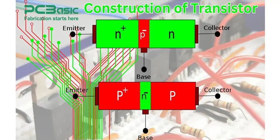
Transistors are usually three layers of semiconductor materials. These semiconductors that can carry each current are materials that come between conductors (e.g., copper) and insulators (such as plastic), even though they sometimes appoint Germanium or Gallium arsenide. The construction process involves "doping" - introducing impurities in the semiconductor to change its electrical properties. This makes either the semiconductor of N-type (with float with additional electrons) or the half-conductor of the p-type (with the electrons removed, with "holes").
The three terminals in a transistor are known as emitter (E), base (B), and collector (C). The base controls the transistor, while the collector acts as a positive lead and emitter as a negative lead. In a BJT, a small forward current flows from the base to the emitter. Since the base sector junction is the other way around, it acts as a barrier. Nevertheless, the forward-biased base-emitter junction allows electrons to pass into the base.
The two main transistor types differ in their construction:
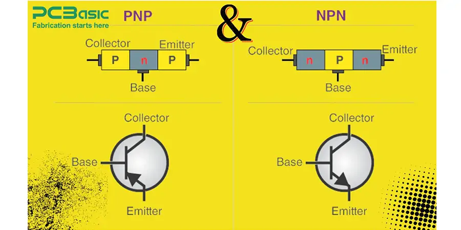
● NPN transistors: One p-type silicon layer (base) sandwiched between two n-type layers (emitter and collector). The majority charge carriers are electrons. Current flows from the collector terminal to the emitter terminal.
● PNP transistors: One n-type semiconductor (base) sandwiched between two p-type layers (emitter and collector). The majority charge carriers are holes. Current flows from the emitter to the collector terminal.
Each layer in a transistor provides a specific purpose. The emitter supplies the charge carriers—electrons in NPN and holes in PNP transistors. The base makes a thin, light dopy between the emitter and the collector. Its primary work is to send the carrier from emitter to collector. The collector collects the carrier sent by the emitter via the base, both larger than both the emitter and base.
The emitter area is strongly doped to increase injection efficiency -ensure that most of the carriers injected into the emitter-base junction cross come from the emitter. In addition, the collector usually surrounds the emitter area, making it almost impossible for electrons injected into the base to escape without collecting it. This design creates the value of α (normal-based power distribution) very close unit, giving the transistor a large β (normal incline power advantage).
Transistors work through the controlled movement of electrical charges in semiconductor intersections. In the core, a transistor acts as both an amplifier and a switch, two basic features that have made it necessary in modern electronics.
The operation of a transistor depends on the application of appropriate voltage for the terminals. For a BJT (bipolar intersection transistor), this is the terminal base, collector, and emitter, which must be identified properly in the transistor pinout to function properly on the device.
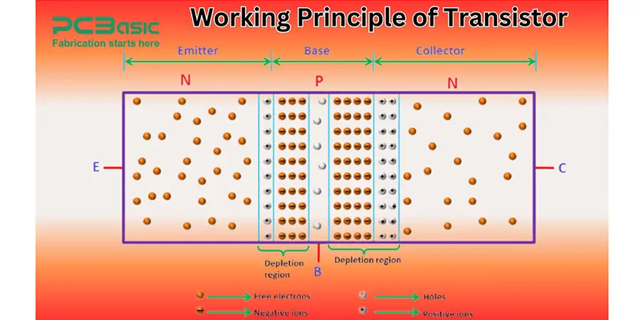
When acting as an amplifier, a transistor takes a small current on a terminal (input) and produces a very large current (output) on the other. This reinforcement is because a small base current controls a very large collector current. In addition, the ratio of these currents is known as current advantage or beta (β), which can range from 20 to high existing types of power transistors to more than 1000.
For amplification, the transistor must work in the "active region", which requires the right bias. This means that the base-emitter junction should be forward biased while the base sector junction remains the reverse biased. Under these conditions, a small signal constitutes a significant improvement output in the collector without deformation.
When used as a switch, the transistor operates between two states: cutting and saturation. In cutting mode, there is no current between the collector and the emitter that corresponds to an open switch. In contrast, in saturation mode, the maximum current flow is similar to a closed switch. This coupling capacity builds a foundation for digital electronics, where transistors form binary conditions that represent 1S and 0S.
For proper operation, it is important to understand the current flow direction. In an NPN transistor, the traditional current flows to the emitter when active from the collector. Alternatively, in the PNP transistor, the current flows from the emitter to the collector.
The relationship between the pinout identity and the work theory cannot be eliminated. The wrong PIN will prevent proper prejudice, impossible or potentially damage to the component. Thus, the correct transistor-pinout identity is fundamentally related to how transistors work.
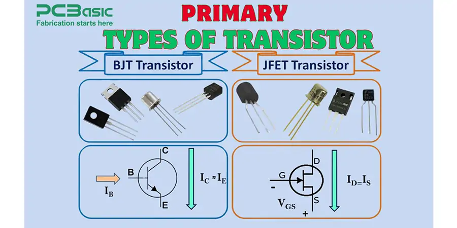
Modern electronics depend on two primary types of transistors, with each having different properties and pinout configurations. Understanding these differences is important for appropriate circuit design and component identity.
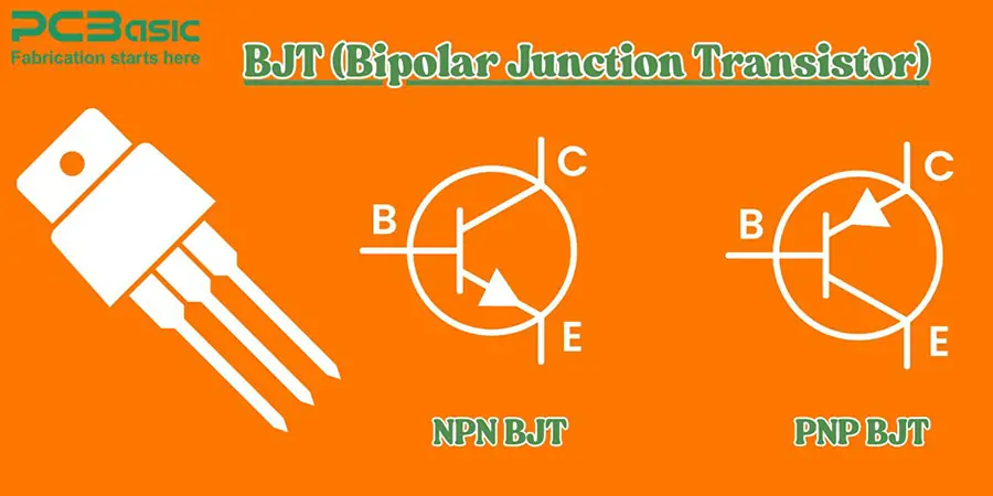
Bipolar Junction transistors use both electrons and electron holes as the charging carrier. Unlike its monarchy colleagues, BJT allows a small stream on a terminal to control a very large current between the other two terminals, enabling reinforcement or switching. These versatile components include two N-type crossings between semi-type and p-type semiconductor areas.
|
Characteristic |
BJT (Bipolar Junction Transistor) |
|
Types |
NPN and PNP |
|
Charge Carriers |
Electrons and Holes |
|
Control Method |
Current-controlled device |
|
Main Applications |
Amplification, Switching, Signal Processing |
2N2222 and BC547 transistors, despite having both NPN types, are different Pinouts. 2N2222 Transistors, A to -18, are available in the Metal Can package, followed by an emitter-base sector Pinout sequence. This package provides high-temperature research capacity.
In contrast, the BC547 transistor, usually placed in a two-92 package, uses a collector base-seminary scheme. Both transistors maintain similar tasks, but these pinout differences are required during circuit mounting to prevent malfunction.
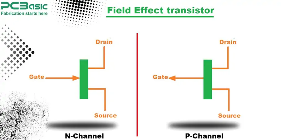
Field power transistors control the power flow via a semiconductor using an electric field. Unlike BJTs, unipolar devices are either electrons (N-channel) or holes (P-channel) but not both. They facilitate three terminals: sources, gates, and drains.
|
Characteristic |
FET (Field-Effect Transistor) |
|
Types |
JFET and MOSFET |
|
Charge Carriers |
Electrons (N-channel) or Holes (P-channel) |
|
Control Method |
Voltage-controlled device |
|
Main Applications |
Amplification, Switching, Power Regulation |
FETs fall into several categories, primarily MOSFETs (metal-oxide-semiconductor FET) and JFETs (junction FET) and you can clear your concepts by reading our blog on BJT vs. MOSFET. In operation, voltage applied to the gate creates an electric field that modifies the channel conductivity between source and drain.
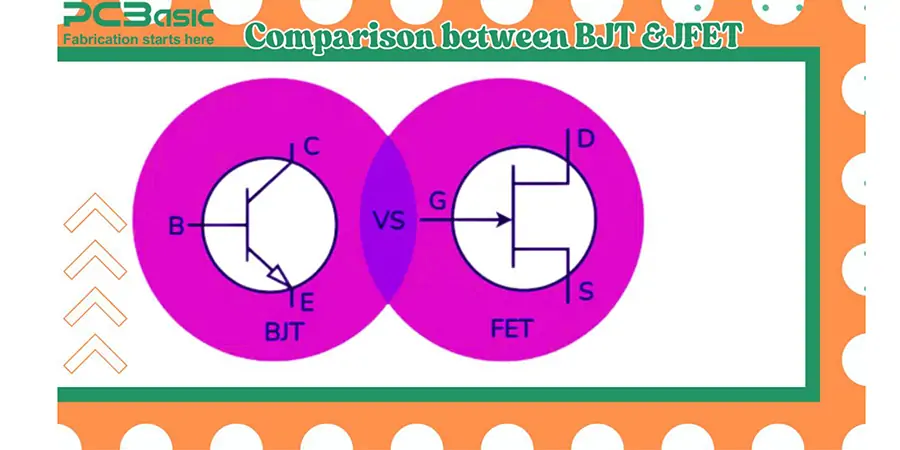
FETs provide many benefits over BJTs, mainly their extraordinarily high input impedance (10^7 to 10^12 ω). This property makes them ideal for entrance stages in multi-style amplifiers. In addition, JFET produces less noise than BJTs, which offers better temperature stability.
Consequently, FETs stand out in applications that require low power consumption and high input impedance. Their voltage-controlled surgery is fundamentally different from the power-controlled nature of BJTs.
|
Characteristic |
NPN Transistor |
PNP Transistor |
|
Current Flow |
From Collector to Emitter |
From Emitter to Collector |
|
Biasing |
The base is positive w.r.t. the emitter |
The base is negative w.r.t. the emitter |
|
Majority Charge Carriers |
Electrons |
Holes |
|
Polarity |
Negative |
Positive |
|
Emitter Arrow Direction |
Points outward |
Points inward |
Nevertheless, FETs present certain limitations, specifically poor frequency response due to high input capacitance and potential damage from static electricity during handling. BJTs, conversely, provide better gain-bandwidth products, making them preferable for specific high-frequency applications.
Transistors serve as the foundation for countless electronic devices, with their pinout configurations playing a crucial role in diverse applications. From simple circuits to complex computing systems, these semiconductor components have changed how we build and use technology.
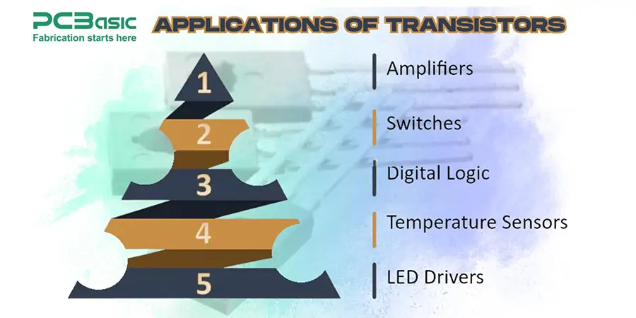
In computing, transistors form the basic building blocks of all digital systems. They create logic gates (AND, OR, and NOT) that combine to build microcontrollers and microprocessors. The transistor-transistor logic (TTL) integrated circuits were standard for processor construction in minicomputers and mainframes before the widespread adoption of VLSI devices. Notably, the more recent Gigatron TTL (2018) demonstrates that processors can still be built entirely with TTL integrated circuits.
As switches, transistors excel at controlling high current loads with low voltage signals. This capacity is especially valuable when microcontrollers need to run engines, relays, or high-power light diodes. Similarly, the H-Brij circuit, which includes four transistors, makes engines rotate both clockwise and counterclockwise, requiring them for robotic applications.
|
Application Type |
Description |
|
Computing |
Form logic gates for microcontrollers and processors |
|
Switching |
Control high-current loads like motors and relays |
|
Amplification |
Boost weak signals in audio and RF systems |
|
Consumer Electronics |
Used in radios, smartphones, and healthcare devices |
Regarding amplification, transistors transform weak signals into stronger ones through various configurations:
● Common emitter arrangement: Ideal for voltage amplification at low frequencies
● Common collector (emitter follower): Perfect for current amplification
● Common base: Functions primarily as a current buffer
Power transistors handle applications requiring high current and voltage, including:
● Audio amplification
● Motor control systems
● Switching circuits
The Darlington amplifier configuration creates exceptionally high current gain by connecting two transistors in sequence. Such arrangements find applications in RF (radio frequency), optic fiber communication, and audio systems.
Similarly, the transistor revolutionized consumer electronics, replacing vacuum tubes in radios and other devices. The first pocket transistor radio (Regency TR -1) appeared in October 1954, followed by the First Transistor Car Radio in 1955.
Mainly includes modern applications computers, smartphones, car systems, health services, robotics, and production equipment. Their continuous relevance dates from their credibility, low costs, and flexibility.
Correctly identifying pins on specific transistor models remains vital for successful circuit design and construction. Let's examine the pinout configurations for several common transistors found in electronic projects.
NPN Transistors
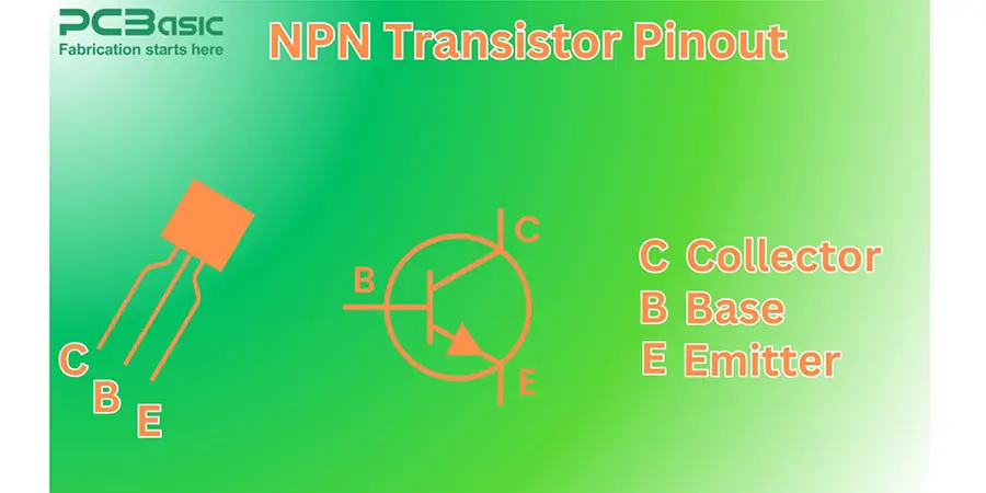
NPN transistors usually follow specific pinout patterns depending on the package type. In TO-92 packages, with the flat side facing you, the pins are numbered 1 to 3 from left to right. However, the specific allocation of the collector, base, and emitter varies from the model. For metal prison transistors, a tab on the ring usually indicates pin orientation. The Emitter Pin is usually located closest to this tab.
|
Characteristic |
NPN Transistor |
|
Current Flow |
Collector to Emitter |
|
Majority Carriers |
Electrons |
|
Biasing |
The base is positive w.r.t. the Emitter |
|
Emitter Arrow |
Points outward |
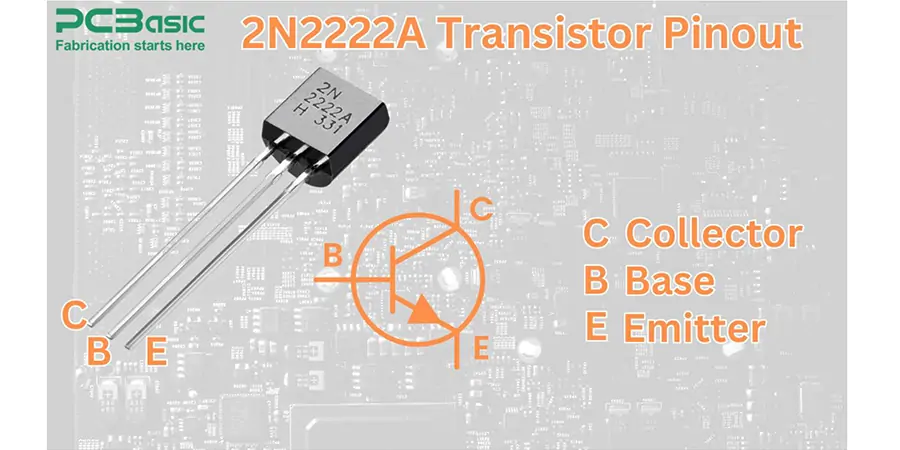
2N2222/2N2222A Transistor comes in two regular packages: TO-92 plastic and -18 metals. For the TO-92 package (P2N2222a), when we look at the flat side with a stick, Pinout: Emitter, base and collector. This confidence facilitates its widespread use in exchange and reinforcement applications. 2N2222 is functionally similar to BC547, but with separate pinout events.
|
Pin Name |
2N2222 Transistor |
|
Pin 1 (Emitter) |
Connects to Ground (-V) |
|
Pin 2 (Base) |
Controls the transistor (Input) |
|
Pin 3 (Collector) |
Connects to Load (+V) |
|
Package Type |
TO-92 (or TO-18 for metal cans) |
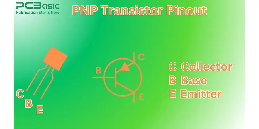
PNP transistors facilitate negative polarity and often different pinout configurations compared to NPN types. Like 2N2907, in PNP transistors, the PIN system usually holds the collector near the package tab. Unlike NPN transistors, where traditional current flows from collector to emitter, the PNP transistor flows from the emitter to the collector. This distinction makes the right PIN identity especially important.
|
Characteristic |
PNP Transistor |
|
Current Flow |
Emitter to Collector |
|
Majority Carriers |
Holes |
|
Biasing |
The base is negative w.r.t. the Emitter |
|
Emitter Arrow |
Points inward |
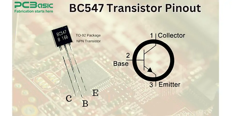
The BC547 transistor, located in a two-92 package, uses a collector-base-seminary configuration when the flat side is seen indicating under the flat side. PIN 1 (Collector) acts as a power input, PIN 2 (base) controls transistor bits, and PIN 3 (emitter) functions as a power output. BC547 has a price value between 110 and 800, so it can handle the collector flows up to 100 mA.
|
Pin Name |
BC547 Transistor |
|
Pin 1 (Collector) |
Connects to Load (+V) |
|
Pin 2 (Base) |
Controls the transistor (Input) |
|
Pin 3 (Emitter) |
Connects to Ground (-V) |
|
Package Type |
TO-92 |
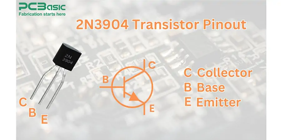
The 2N3904 NPN transistor, also in a TO-92 package, features an Emitter-Base-Collector arrangement. The emitter (pin 1) drains current, the base (pin 2) controls biasing, and the collector (pin 3) serves as the current input. With a gain of 300 and the ability to handle collector currents up to 200mA, it's ideal for small signal amplification and switching applications.
|
Pin Name |
2N3904 Transistor |
|
Pin 1 (Emitter) |
Connects to Ground (-V) |
|
Pin 2 (Base) |
Controls the transistor (Input) |
|
Pin 3 (Collector) |
Connects to Load (+V) |
|
Package Type |
TO-92 |
Understanding transistor pinouts is essential for a good digital initiative. Throughout this guide, we explored various factors of transistors, from simple identification strategies to specific model configurations. This know-how helps save you circuit malfunctions and component harm whilst enabling the right implementation in diverse packages.
The manual blanketed critical distinctions among BJT and FET transistors, their working concepts, and common applications. We tested famous models, such as the 2N2222, BC547, and 2N3904, detailing their specific pinout preparations. This information proves treasured whether running with simple amplifier circuits or complex computing structures. Mastering transistor pinouts calls for exercise and attention to detail. For particular specs of common transistors, just like the 2N2222, visit our comprehensive guide at PCBasic's transistor pinout aid of 2N2222.
Armed with this know-how, you can expectantly tackle electronic projects related to transistors. Remember to seek advice from manufacturer datasheets, verify package sorts, and double-check pin configurations before circuit assembly. These practices, blended with the understanding gained from this manual, will result in a hit implementation of transistor-based total circuits for your future projects.

Assembly Enquiry
Instant Quote
Phone contact

+86-755-27218592
In addition, we've prepared a Help Center. We recommend checking it before reaching out, as your question and its answer may already be clearly explained there.
Wechat Support

In addition, we've prepared a Help Center. We recommend checking it before reaching out, as your question and its answer may already be clearly explained there.
WhatsApp Support

In addition, we've prepared a Help Center. We recommend checking it before reaching out, as your question and its answer may already be clearly explained there.