Global high-mix volume high-speed PCBA manufacturer
9:00 -18:00, Mon. - Fri. (GMT+8)
9:00 -12:00, Sat. (GMT+8)
(Except Chinese public holidays)
Global high-mix volume high-speed PCBA manufacturer
9:00 -18:00, Mon. - Fri. (GMT+8)
9:00 -12:00, Sat. (GMT+8)
(Except Chinese public holidays)
HomePage > Blog > Knowledge Base > What is Through-hole Assembly?
Through-hole assembly is a relatively traditional PCB assembly method. However, it is still widely used up to now because it is strong, durable and highly reliable. Its approach is actually very simple. Just insert the pins of the through-hole components into the pre-drilled through holes on the circuit board and then solder and fix them on the back.
This technology is particularly suitable for industries such as aerospace, automobiles, power, and military, as these devices often have to deal with extreme environments like high temperatures and vibrations. Using through-hole assembly will be more stable and safer. The circuit boards (PCBs) manufactured with through-hole technology are more robust compared to surface mount technology (SMT) and are also more convenient for later maintenance or component replacement.
Now, let's take a look together at the specific differences, advantages of through-hole assembly and compare through-hole vs surface mount technologies.
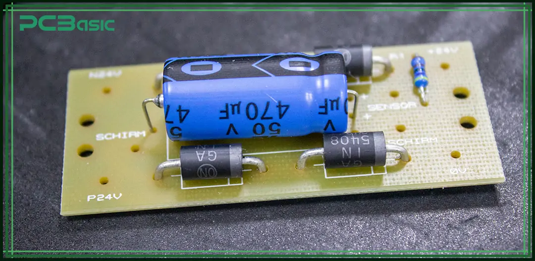
In modern electronics, the term through-hole refers specifically to these small, drilled openings in a PCB through which leads of electronic components can be inserted. These holes allow electrical connections from layer to layer of the printed circuit board (PCB).
These holes are filled with components with long leads, ensuring both mechanical stability and an electrical connection between the PCB layers. This process is different from, for example, the surface mount assembling method, which could be soldered on the PCB surface without any drilling.
Through-hole components are those electronic parts with long leads. These leads need to be inserted into the pre-drilled holes on the circuit board and then soldered and fixed on the back. Although they have different shapes and sizes, they all have one thing in common - they need to be installed through circuit boards.
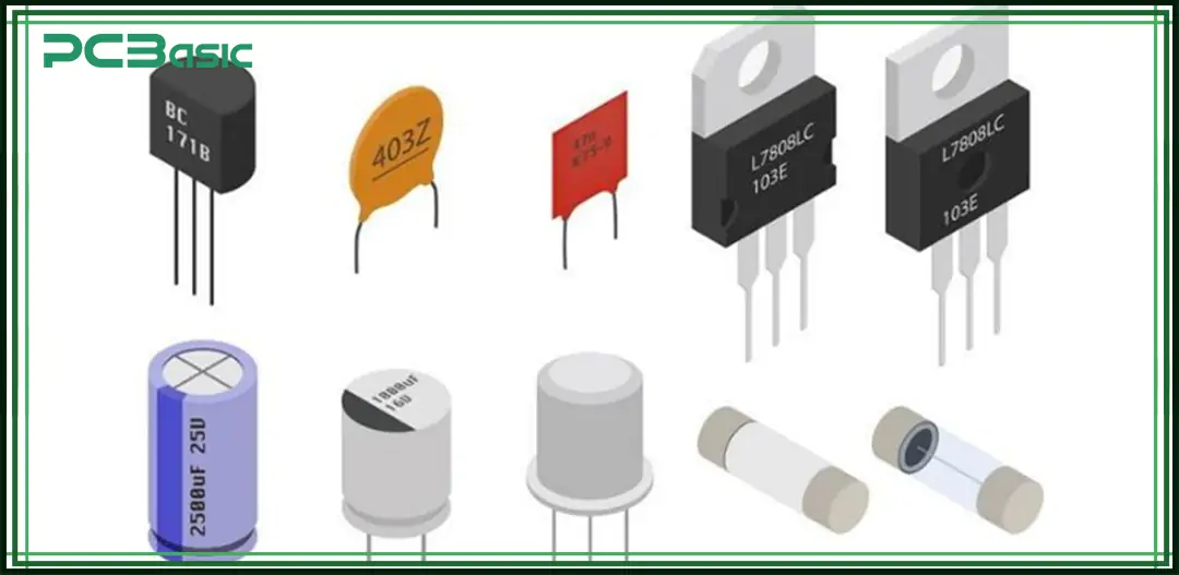
Common through-hole components include:
• Resistors – The most common ones are small cylindrical shapes with metal legs on both ends
• Capacitors – Especially electrolytic types, look like tiny cans
• Inductors – Coil-shaped parts, often used in power or wireless devices
• Diodes and LEDs – Small parts that control current direction or light up
• Connectors and headers – Used for plugging in wires or connecting other modules
• Transistors and IC chips – Black rectangular parts with multiple legs, good for experiments
Through-hole assembly involves inserting leads of components into holes drilled in the PCB and soldering them to secure robust connections. There is a critical assembly phase in PCB production, and the method is still widely used in electrically demanding applications.
Comparatively, through-hole assembly is better for high-stress applications since it offers stronger mechanical connections. It could also accommodate components with larger tolerances, making it suitable for some rugged environments.
Isn't surface mount technology (SMT) all the rage now? Then why use through-hole assembly?
By the 1970s, the technology of through-hole assembly was widely embraced and it was the most common practice throughout the assembly of printed circuit boards for several years. The use of surface mount technology may have progressed over time but through-hole techniques are still used in certain applications as they are more reliable. With regards to through-hole assembly, some of its defining characteristics are:
• Stronger Connections: Provides long-lasting joints with good resistance to mechanical load, so it is suitable for a high-vibration environment.
• Ideal for Prototyping and Testing: Prototypes can easily be built since the structures can be modified, changed, or fixed when in the stage of design.
• Efficient for High-Power Components: Supports large, high-power electronic components that require security.
• Reliable Multi-Layer Integration: Allows interconnection of multiple PCB layers and thus performs reliably in numerous challenging circuits.
• Built for Extreme Environments: It gives excellent performance in tough industrial or environmental environments while ensuring long-term operation.
Although through-hole assembly provides many benefits, it is very tedious and more labor-intensive compared to SMT. It thus becomes impractical for high-density compact design circuits.
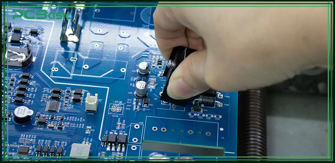
The through-hole assembly process follows a step-by-step process to ensure reliable connections with durable PCBs. Here are some crucial steps:
The PCB layout must have a suitable through-hole size and proper placement to allow for easy and effective insertion of components, as well as to accommodate the assembly.
Precise holes are drilled into the PCB using advanced machinery by the design specifications to promote proper alignment and structural integrity.
Holes that have been drilled are plated with conductive materials (such as copper) to create electrical connections between the layers of the PCB, as well as to make the holes more durable.
 About PCBasic
Time is money in your projects – and PCBasic gets it. PCBasic is a PCB assembly company that delivers fast, flawless results every time. Our comprehensive PCB assembly services include expert engineering support at every step, ensuring top quality in every board. As a leading PCB assembly manufacturer, we provide a one-stop solution that streamlines your supply chain. Partner with our advanced PCB prototype factory for quick turnarounds and superior results you can trust.
Insertion of components into the plated holes by hand or automation, ensuring components are positioned and oriented correctly for best performance.
The PCB is moved through a wave of molten solder, which solders all the pins of components together tightly so solder joints are strong and uniform.
The assembled PCB undergoes an examination and a test for mechanical stability and electrical functionality to identify potential defects, which can then be corrected.
The tested PCB is assembled into the final product or system, marking the end of the manufacturing process for reliable use.
In PCB manufacturing, there are two main methods: through-hole assembly and surface mount technology (SMT). Each has its own advantages, depending on the application. Through-hole assembly is known for its rugged connections, which make it suitable for high-stress environments. SMT, on the other hand, is preferred in many applications due to its efficiency in manufacturing, cost-effectiveness, and compatibility with compact designs. Here is a detailed comparison to help you understand the two:
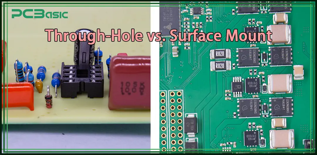
• Connection Strength: Due to stronger connections through-hole assembly, PCBs are applicable to high-stress applications. SMT provides suitable strength for low-stress conditions but is less persistent under vibration.
• Component Size: Through-hole assembly allows for larger components, like connectors, to be supported, while the SMT assembly is designed for smaller, lighter components and, thus, allows compact device designs.
• PCB Size: Through hole requires more PCB space due to the requirement of drilled holes and diminishes circuit density. The SMT assembly offers higher-density designs by placing their parts on the board's surface and maximizing the available space usage.
• Production Speed: On the other hand, the through-hole assembly takes a lot more time because it involves manual processes, while the SMT is faster and more automatic, thus leading to quick, high-volume production.
• Cost: More labour-intensive and also adds up more steps; through-hole assembly cost is comparatively higher. Surface mount technology is cost effective usually for huge mass production.
• Application: Industries such as aerospace, automotive, and military rely on through-hole technology for its mechanical strength and reliability in harsh environments.
• Repairability: The modification is easier in Through Hole assembly because of larger components and easy access to solder joins and the SMT is very difficult to repair because of smaller components and huge density.
Here is a clear comparison table, making it easier to understand the differences between through-hole and surface mount technology in PCB assembly:
|
Comparison Aspect |
Through-Hole Assembly |
Surface Mount Technology (SMT) |
|
Connection Strength |
Stronger, ideal for high-stress and vibration environments |
Moderate strength, less reliable under vibration |
|
Component Size |
Supports larger components |
Designed for smaller, lightweight components |
|
PCB Size Efficiency |
Requires drilled holes, uses more board space, lower circuit density |
Components mounted on surface, enables compact, high-density PCB designs |
|
Production Speed |
Slower due to manual processes |
Faster, highly automated, suitable for mass production |
|
Cost |
More labor-intensive, higher cost |
Cost-effective, especially for large-volume manufacturing |
|
Application Fields |
Aerospace, automotive, military (demand high mechanical strength and reliability) |
Consumer electronics, computers, mobile devices (where compactness is critical) |
|
Repairability |
Easier to modify and repair due to larger components and accessible solder joints |
More difficult to repair due to small size and high component density |
After having a look at these points, a manufacturer feels comfortable and easy while choosing the right assembly method according to the need of design price and performance requirements.
In conclusion, the through-hole assembly has its specific niches in electronic manufacturing where it is the most beneficial, and this is because it offers unique advantages. On the other hand, when dealing with compact, high-density, and low-cost designs, it is SMT that captures the market. In circumstances that demand mechanical strength, through-hole technology still works best where longevity and reliability are vital.
Due to its robustness, it is also the preferred technology in construction where the components would be subjected to shocks, vibrations, and other tough environmental conditions.
One way of making better decisions in a manufacturing set-up is to know the positives or negatives of both through-hole assembly and surface mount technology. Businesses employing a smart combination of both technologies would be able to optimize their production processes, balancing prices, performance, and reliability for producing advanced, durable, and efficient electronic devices to meet a wide application and industrial portfolio.
Assembly Enquiry
Instant Quote
Phone contact

+86-755-27218592
In addition, we've prepared a Help Center. We recommend checking it before reaching out, as your question and its answer may already be clearly explained there.
Wechat Support

In addition, we've prepared a Help Center. We recommend checking it before reaching out, as your question and its answer may already be clearly explained there.
WhatsApp Support

In addition, we've prepared a Help Center. We recommend checking it before reaching out, as your question and its answer may already be clearly explained there.