Global high-mix volume high-speed PCBA manufacturer
9:00 -18:00, Mon. - Fri. (GMT+8)
9:00 -12:00, Sat. (GMT+8)
(Except Chinese public holidays)
Global high-mix volume high-speed PCBA manufacturer
9:00 -18:00, Mon. - Fri. (GMT+8)
9:00 -12:00, Sat. (GMT+8)
(Except Chinese public holidays)
HomePage > Blog > Knowledge Base > What Is SMT Assembly?
With the global demand for more heat-tolerant and lightweight electronics such as laptops and smartphones, small and large-scale manufacturers have continued to rely on SMT assembly to mass produce such products. The market size for this technology has been predicted to increase by more than 8.1% from 2023 to 2032.
Then, what is SMT assembly? How does it differ from traditional assembly methods? In this blog, we will explain in detail what SMT is, the SMT process, and the advantages of using SMT PCB assembly.
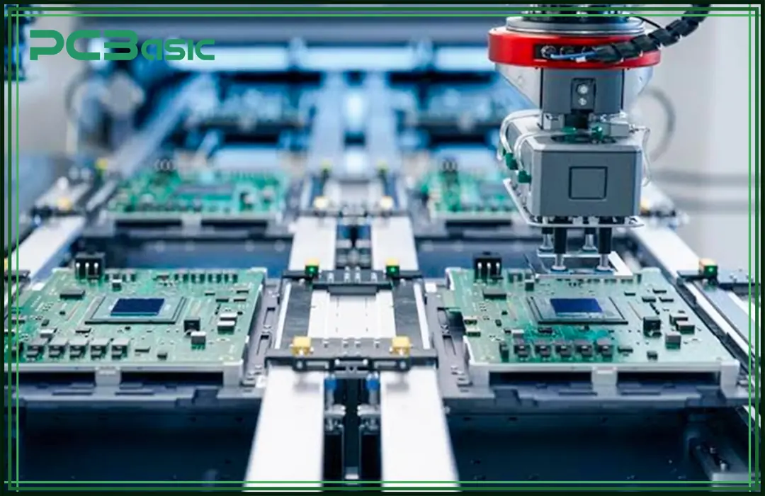
SMT stands for surface mount technology. It is a technique of joining smaller electronic components.
SMT assembly means assembling SMD components, such as diodes, resistors, and capacitors, onto a laminate substrate (PCB). This design allows for compact placement of components, enabling efficient use of PCB space.
The role of SMT assembly in the current industry is enormous. For example, It decreases the device sizes by more than 50%. In addition, it enhances the heat dissipation and reduces the power consumption of the devices.
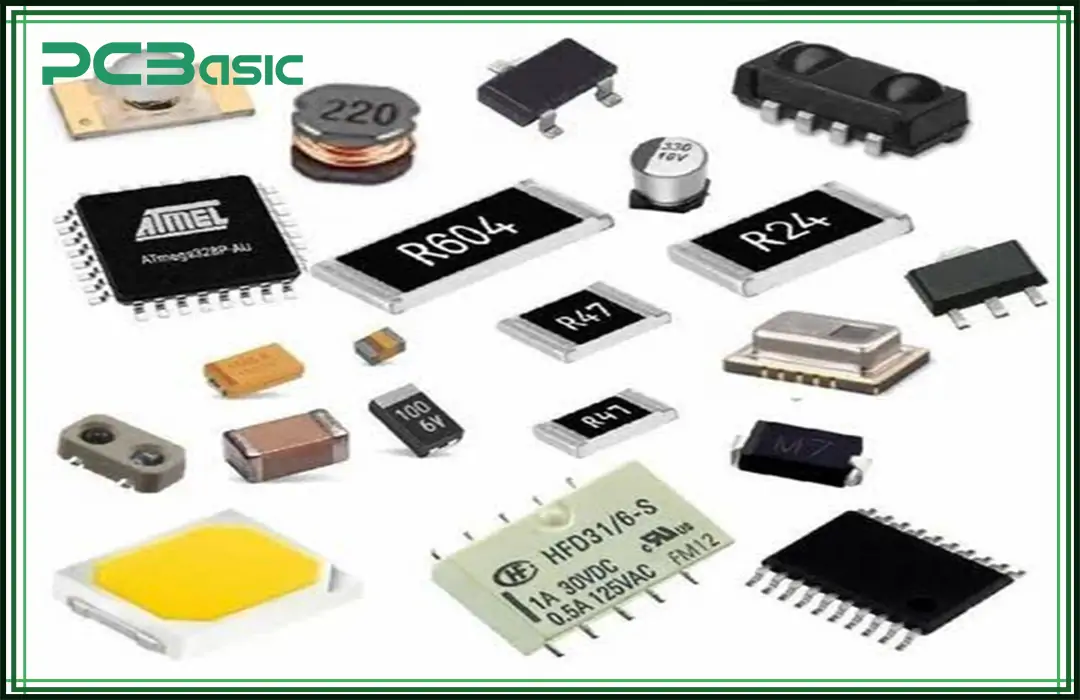
SMD stands for surface mount devices. They are the components that are mounted or attached to a PCB. They have short terminals which grip them very firmly to the plane of the circuit board. Some examples are capacitors, LEDs, transistors, and resistors.
There are six main steps to follow when carrying out SMT assembling of components. They are:
Layout design consists of finding a usable space on the board on which the SMDs can fit themselves. In order to guarantee that each component bonds correctly, calculations are made to determine a fixed board size, shape, and thickness. Afterward, technicians decide on the optimal positions and orientations with the components.
The fabrication starts with selecting suitable epoxy-based silica materials like the FR4 and FR5. After that, the printed board layer is fabricated. Next, the copper foil layer is created using etching and laminating techniques, followed by the silkscreen layer, which is applied using silkscreen printing and ink curing.
After the layers align properly, molten copper is deposited on the previously designed layout on the PCB, and excess copper is removed along the board paths.
Materials selection is incorporated in this procedure, for example, deciding the best materials, such as stainless steel, for the rendering. After that, the stencil is created using laser cutting or chemical etching.
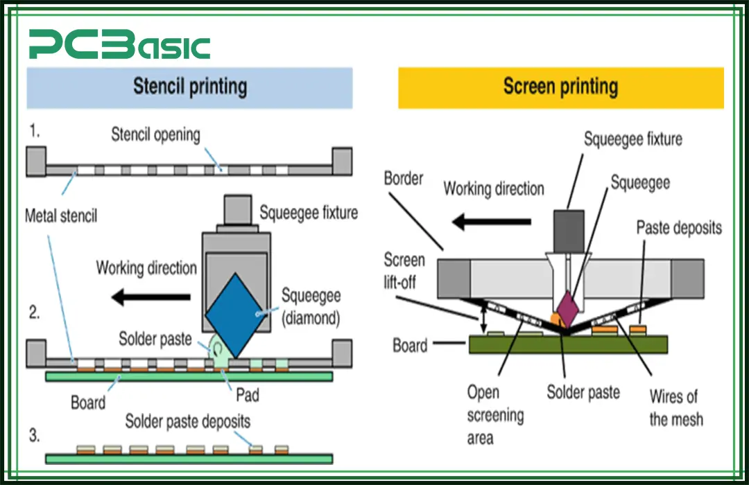
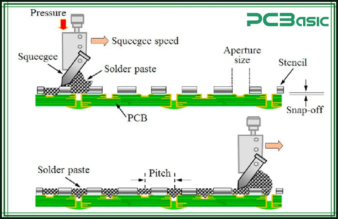
This includes pre-heating the solder to a paste prior to its top-coating on the PCB at a temperature ranging from 220 to 250 °C. Subsequently, the paste is stamped onto the PCB through a stencil. At the end of the process, the board and paste are allowed to sit at room temperature.
It focuses on the application of pick and place machines to attach the circuit modules to the board. Before putting the pieces in the right place they are sorted in reels or trays. Following this, the machine lifts each part and drops them into the correct position.
Then, the operator performs a visual check to ensure all components are correctly positioned.
This is done to check the integrity of the assembled elements. For this, operators employ either Automated X-ray Inspection (AXI) or Automated Optical Inspection (AOI) machines to check the soldered joints.
Designers conduct this test to detect defects such as solder bridges or incorrect positioning of the circuit devices.
Such an approach is taken to detoxify the PCB by exploiting surface-cleaning techniques such as ultrasonic cleaning or cleaning with a solvent. Isopropanol or deionized water is employed to wipe the board surfaces for this purpose.
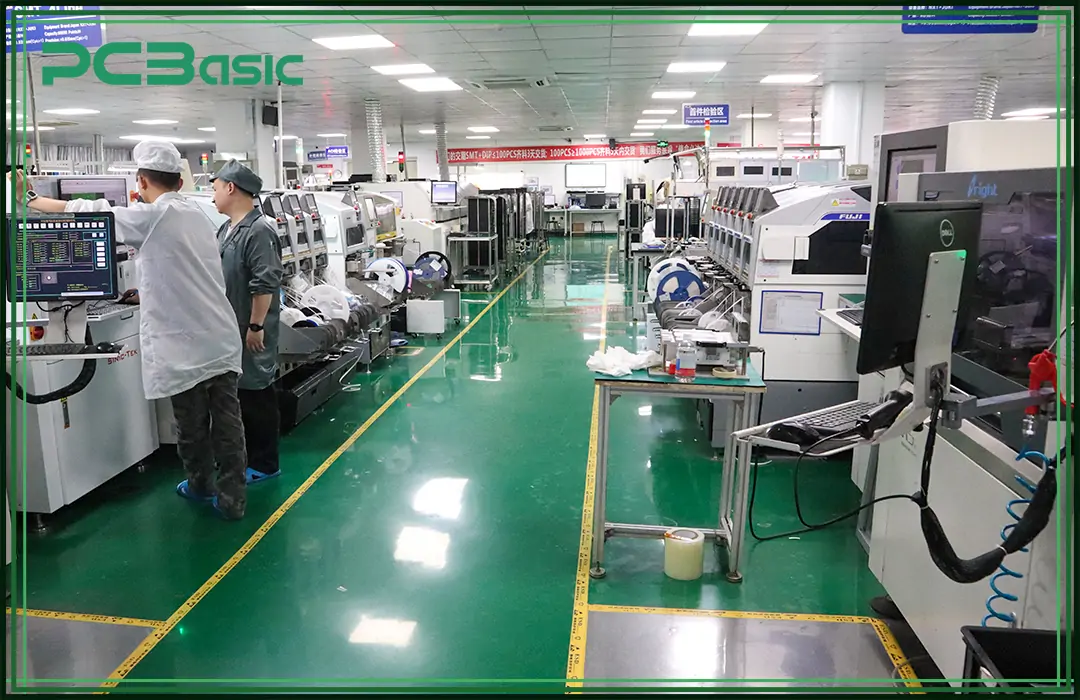
In industry, manufacturers are generally keen to apply this technology for the mass production of components because of the many advantages that it provides. A few of these merits are discussed below.
SMT assembly enables better thermal management because it reduces the size of the SMDs attached to the circuit board. The assembling lines have thermal pads, vias, and other heat reduction techniques to balance the heat dissipation in the system.
SMT technology lowers labor costs through automated production units that reduce product quality problems caused by human mistakes.
Thanks to the SMT assembly, it is feasible to place intricate patterns of devices over the board as the components can be positioned into a more compact area of the board.
Due to the high adhesion of the mounted devices on the surface of the PCB, which prevents damage caused by shock, thermal, and mechanical stress, the SMT attaching process makes highly durable PCBs possible.
Surface-mount techniques take up less room than conventional through-hole technology. The main reason is the reduction in the size of Surface Mount Devices (SMDs) that can be directly attached to PCB without any holes.
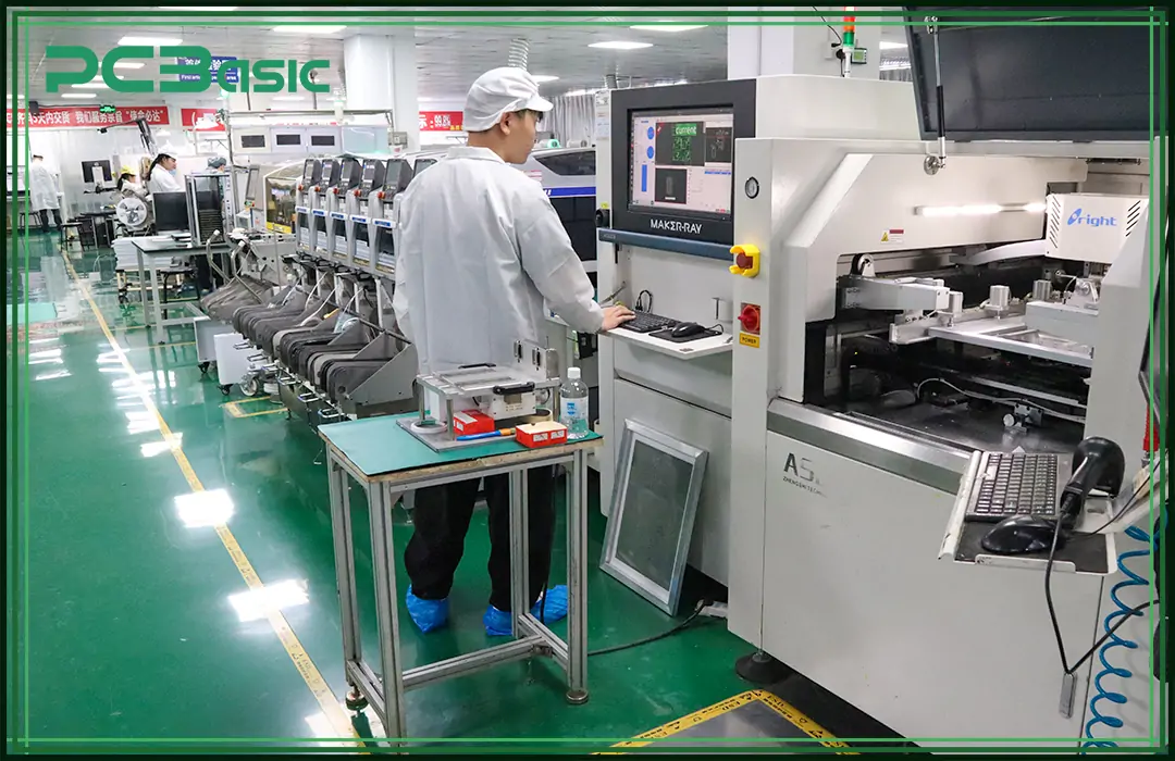
Although used daily within the electronics industry, SMT technology is still associated with problems/difficulties, making the process undesirable for small-scale manufacturers. Some of these challenges include:
It is hard to repair most SMT circuits because of the compact mounting of components. Because of the high packing density, there is very limited space for technicians to work on the replacement of faulty components. Due to this, repair work becomes time-consuming and expensive.
Initial equipment cost and training of staff are both very high when setting up an SMT production line. Due to this high capital intensity, the technology is less appealing for small businesses operating on limited budgets.
The smaller electronic components used in SMT are increasing the challenges for technicians carrying out visual inspection, compared to traditional through-hole technology.
Several SMT devices are susceptible to thermal effects during their fabrication, which in turn results in a shorter lifespan.
The presence of solder in the SMT fabrication process creates various problems, including inadequate wetting, oxidation, and misalignment of components. These defects can result in electrical connectivity issues that degrade the integrity of the final product.
Looking for reliable PCB assembly services? At PCBasic, we specialize in SMT PCB assembly, providing high-quality SMT assembly solutions for various industries. Our advanced SMT process ensures precision, efficiency, and cost-effectiveness.
With PCBasic, you get:
✔ High-speed automated SMT assembly
✔ Reliable sourcing of SMD components
✔ Stringent quality control in every SMT PCB assembly
✔ Affordable PCB assembly services with a global supply chain
The advantages of SMT assembly, such as space-saving and good operational performance, cannot be ignored despite the problems it raises. In particular, the high cost of repairs makes the system very expensive for small companies. In spite of this, SMT is still the preferred choice for electronics manufacturing, even with the scaling up of manufacturing energy-saving devices.
For students, engineers, or manufacturers in training, knowing both the benefits and drawbacks of SMT is critical to effectively utilize the technology.
Assembly Enquiry
Instant Quote
Phone contact

+86-755-27218592
In addition, we've prepared a Help Center. We recommend checking it before reaching out, as your question and its answer may already be clearly explained there.
Wechat Support

In addition, we've prepared a Help Center. We recommend checking it before reaching out, as your question and its answer may already be clearly explained there.
WhatsApp Support

In addition, we've prepared a Help Center. We recommend checking it before reaching out, as your question and its answer may already be clearly explained there.