Global high-mix volume high-speed Shenzhen PCBA manufacturer

Ru
9:00 -18:00, Mon. - Fri. (GMT+8)
9:00 -12:00, Sat. (GMT+8)
(Except Chinese public holidays)


Global high-mix volume high-speed Shenzhen PCBA manufacturer

Ru
9:00 -18:00, Mon. - Fri. (GMT+8)
9:00 -12:00, Sat. (GMT+8)
(Except Chinese public holidays)


HomePage > Blog > Knowledge Base > Gold Fingers – PCB
The advancement of printed circuit board (PCB) technology is driving the improvement and innovation of device performance, among which the PCB Goldfingers is a crucial connection solution, assuming the key role of transmitting data and power, ensuring the complex interaction and efficient operation of modern electronic equipment. Next, this article will have an in-depth discussion of gold fingers, introducing the definition of gold fingers, design requirements, production process and its core role in different applications; I hope you can learn something after reading.
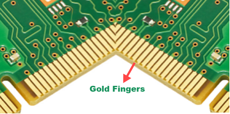
PCB gold fingers are a row of narrow, long and thin metal contact areas located on the edge of a printed circuit board (PCB), as shown below:

Because the contacts shown in the figure are long and narrow, like fingers, and are covered with a layer of gold (the metal covered is usually gold, which is used to improve electrical conductivity and corrosion resistance), they are called "gold fingers." These metal contacts are critical to electronic devices because they can provide a physical connection (usually a slot connection) between hardware devices, allowing data, electrical signals, and power to be transferred between different devices or boards. It is widely used, not only for the motherboard connection inside the electronic equipment, such as expansion card, but also as an important physical connection interface is widely used in industrial equipment and communication equipment.
Goldfingers has been around since the early 20th century in electronics manufacturing. Later, with the rapid development of the electronics industry and the widespread use of computers and mobile communication equipment, the design and application of Goldfingers became more and more mature, and the relevant standards were gradually established. Here are some key criteria:
|
Standards |
Requirements |
|
IPC-4552 |
Specifies requirements for Electroless Nickel/Immersion Gold (ENIG) plating for printed circuit board surface treatment |
|
IPC-4556 |
Covers specifications for electroplated hard gold |
|
ASTM B488 |
Provides specifications for gold electroplating, including type, thickness, and purity of the gold plating process |
|
UL Certification |
Materials and manufacturing quality of gold fingers must meet UL standards |
|
ISO Standards (ISO 9001) |
Standards for quality management and continuous improvement processes for gold fingers |
|
RoHS and REACH |
Imposes strict restrictions on the use of materials (such as nickel, gold, etc.) in the production of gold fingers |
|
MIL |
Specifies the performance and durability of gold fingers in extreme environments |
The design and manufacture of gold fingers must comply with relevant standards such as IPC to ensure that the manufactured gold fingers can maintain consistency and interchangeability on a global scale and improve the reliability and market competitiveness of the products.
1. Thickness
When designing the gold fingers, the length, width and position of the gold fingers should be precisely determined according to the interface specifications of the target device. It usually requires a layer of gold plating to improve electrical conductivity and corrosion resistance (a layer of nickel is usually plated before gold plating to enhance the adhesion and wear resistance of the gold layer), and the thickness is usually between 3 microns and 50 microns. PCBasic can tailor the design to the different uses and applications of the customer's products, and this customization allows each product to perform optimally in its specific operating environment while also extending the service life of the product.
2. Chamfer
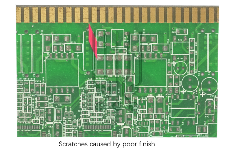
The edge of the gold fingers usually needs to be chamfered or rounded to ensure that the connector can be inserted quickly and to prevent the gold fingers from scratching the card slot or exposing the copper during insertion and removal. (This step is usually done after the pad cover is coated and before the surface treatment.)
3. Location
The distance between the gold fingers and the PTH hole should be 1 mm, while the minimum distance between the gold fingers and the edge of the board should be 0.5 mm, which can reduce the probability of board failure. And do not place any pads, holes, or screen prints in the gold fingers area, as these elements can cause the gold fingers to be damaged or the electrical connection to be poor during insertion and removal.
4. Electrical and mechanical properties
The electrical properties and mechanical strength of gold fingers should be considered in the design to ensure that they can withstand frequent physical insertion and removal while meeting electrical requirements.
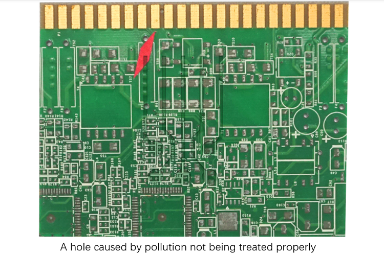
5. Pollution

Measures should be taken during the design and manufacturing process to prevent oil, dust, and other pollutants from adhering to the gold fingers. Otherwise, it will have adverse effects (such as holes) and affect its electrical performance.

The surface treatment of the gold fingers is an important step in its design and manufacture, and with the right surface treatment technology, the overall performance and durability of the gold fingers can be significantly improved, ensuring its efficient and reliable connection in a variety of applications. Goldfingers surface treatment methods include Electroplated Hard Gold, electroplated soft Gold, ENIG, ENEPIG and selective plating. The two most used are Electroplated Hard Gold and ENIG. Here's a table about them:
|
Feature |
Hard Gold Plating |
Electroless Nickel Immersion Gold (ENIG) |
|
Wear Resistance |
High, suitable for applications requiring frequent plugging and unplugging |
Lower than hard gold, not suitable for frequent plugging |
|
Corrosion Resistance |
Excellent, can resist environmental corrosion |
Very good, provides long-term corrosion protection |
|
Electrical Performance |
Good, suitable for applications needing reliable electrical connections |
Excellent, smooth gold layer provides superior electrical contact |
|
Cost |
Higher, due to the thicker gold layer |
Lower, thinner gold layer, but the cost of nickel layer also needs consideration |
|
Application |
Suitable for high wear and mechanical strength requirements, such as military and aerospace equipment connections |
Suitable for fine electronic devices and high-density interconnect (HDI) boards |
|
Solderability |
Good, but soldering temperature and time control are necessary |
Excellent, ENIG is solder-friendly, widely used in SMT soldering |
|
Surface Smoothness |
May have slight unevenness due to electroplating, but usually does not affect performance |
Very smooth, suitable for mounting precision components |
The Goldfingers is essential for a stable and reliable physical connection of electronic devices. In its design and manufacturing process, it is necessary to strictly follow the corresponding industry standards, so as to ensure that the production of gold fingers in the world to maintain consistency and interchangeability. If you have any questions, please feel free to contact us!

Assembly Enquiry
Instant Quote