
Global high-mix volume high-speed PCBA manufacturer
9:00 -18:00, Mon. - Fri. (GMT+8)
9:00 -12:00, Sat. (GMT+8)
(Except Chinese public holidays)





HomePage > Blog > Knowledge Base > Edge Computing PCB Assembly: Design, Manufacturing, and Reliability Solutions for AI Hardware
Table of Contents
1. What is Edge Computing PCB Assembly?
2. Why Edge Computing PCBs Require Specialized Design
3. PCB Design and Assembly Considerations for Edge Computing PCB Assembly
4. Typical Applications of Edge Computing PCB Assembly
5. How to Choose an Edge Computing PCB Assembly Partner
Artificial intelligence (AI), Industrial IoT, and smart automation have completely changed the way we deal with data. Today, many AI-enabled and IoT devices process at least part of their data locally instead of sending all raw data to centralized cloud servers. This concept, known as edge computing, can offer faster data processing, better data privacy, and quicker decision-making. The performance of many edge computing devices depends on reliable edge computing PCB design and assembly.
With the number of edge AI applications constantly increasing in manufacturing, healthcare, transportation, and smart cities industries, the requirements for PCBs have become significantly higher. The design and manufacturing process is much more complicated than in the case of regular boards.
The following is a comprehensive guide to edge computing PCB assembly, its design principles, assembly challenges, use cases, and ways of choosing an appropriate manufacturer for reliable edge computing solutions.
Edge computing PCB assembly is the term that stands for the process of mounting, soldering, inspecting, and testing electronic components on PCBs used in edge computing hardware. Unlike regular electronics, such systems analyze data within a device instead of performing analysis via cloud computing. It helps achieve faster processing, save bandwidth, and improve data privacy by keeping more data closer to its source.
A typical edge computing PCBA consists of powerful processors, accelerators for AI tasks, memory units, components for wireless connections, power circuits, and multiple interfaces for sensors. Since many of these assemblies are designed to operate continuously in industrial or outdoor conditions, high reliability is one of the most crucial design aspects.
In light of the evolution of edge AI PCB Assembly, modern manufacturers have to achieve better tolerances and assemble more complicated boards. Today, high-density routing, fine-pitch BGAs, embedded processors, and other innovations are increasingly used in high-performance edge computing devices.
|
Aspect |
Standard PCB Assembly |
Edge Computing PCB Assembly |
|
Processing Power |
Basic microcontrollers |
AI processors, NPUs, and high-performance CPUs |
|
Data Processing |
Application-dependent |
Real-time local processing |
|
PCB Complexity |
Medium |
High-density multilayer designs |
|
Thermal Requirements |
Moderate |
Advanced heat management |
|
Reliability |
Consumer-grade |
Industrial and mission-critical reliability |
|
Testing |
Standard functional testing |
Comprehensive functional, thermal, and reliability validation |
Edge computing PCB fabrication demands sophisticated engineering that ensures good signal integrity, power delivery, electromagnetic interference control, and thermal management within compact designs. Considering the fact that industrial edge computers may run for many years, they incorporate longevity components and follow strict quality assurance practices.
Unlike traditional electronic boards, AI edge computing PCB products have to perform data processing right there while keeping latency and reliability low and minimizing power usage. It means that these systems are typically used in places such as factories, transportation, healthcare facilities, or outside buildings, where performance cannot be compromised in any way. Here are some reasons why edge computing PCBs are more challenging compared to normal PCB assemblies.
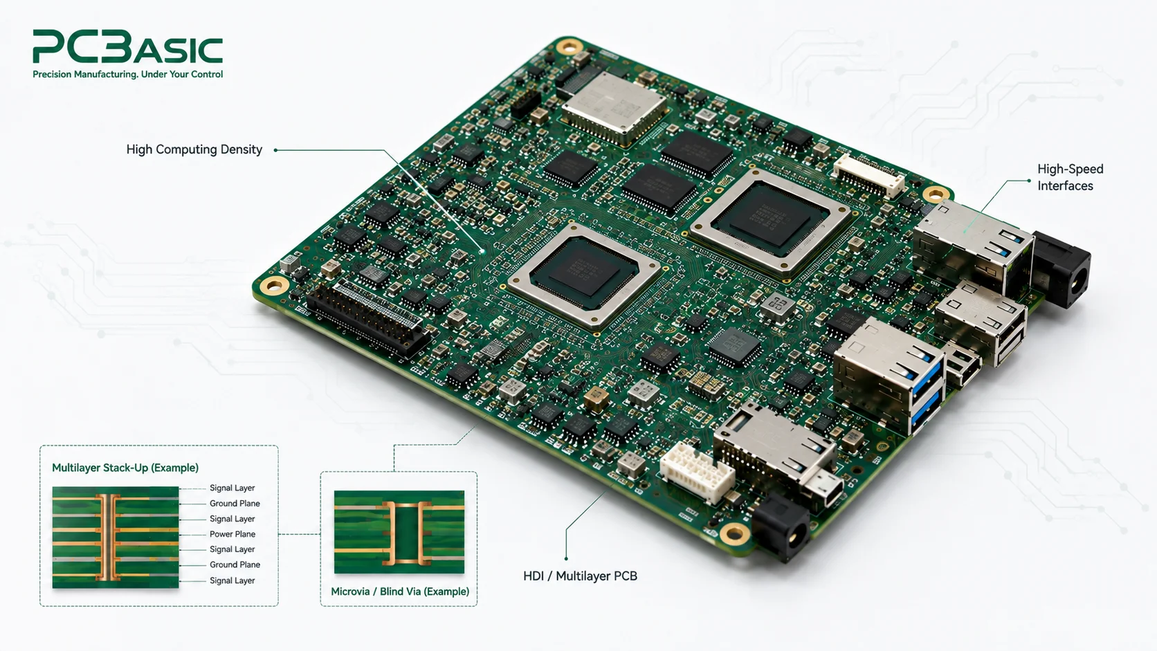
Edge computing PCB designs feature complex hardware components such as AI processors, GPUs, memory chips, wireless modules, sensors, and power management circuitry all located on one board. The increased component density creates routing challenges for PCB designers.
The AI hardware PCB assembly usually incorporates high-speed interfaces such as PCIe, USB 3.0, Ethernet, MIPI, and DDR memory bus. High-speed interfaces have special design considerations that include controlled impedance routing, trace length matching, and careful layer assignment in order not to degrade the signal.
High-density interconnect (HDI) technology is a common feature in many edge AI PCB assembly projects. Design elements like microvia, blind via, buried via, and fine-pitch BGA help to squeeze maximum performance into a minimal size of the board.
Many industrial and outdoor edge computing devices operate in an environment with extreme temperatures, unlike normal office conditions. There can be industrial automation equipment, transportation devices, agriculture sensors, and surveillance systems that may be designed for extended temperature ranges such as -40°C to +85°C.
Due to these requirements, each high-reliability edge computing PCBA should feature industrial components that will ensure stable operation under continuous thermal stress.
The same applies to the choice of PCB materials since they should be thermally stable, resist humidity, and have good mechanical strength properties. It is crucial to choose a correct PCB substrate that ensures minimal expansion, twisting, and other reliability issues.
With the increasing speed of processing, the issue of signal integrity is becoming increasingly complicated. Due to high-speed communication between the processor, memory, and peripherals, there is a significant generation of electromagnetic interference (EMI) that can have negative consequences for the system.
Proper routing of signals, as well as power integrity, is critical for an AI edge computing PCB. Proper grounding, differential pair routing, shielding, and correct stack-up ensure good signal integrity. Similarly, it is crucial to provide a stable voltage to the processor to prevent its unexpected resets.
As opposed to consumer electronics that become outdated every couple of years, edge computing hardware may work for decades at a time. Machinery, medical devices, and intelligent systems need hardware that will be capable of working constantly without any interruptions.
That is why the edge computing PCB assembly manufacturer needs to take into account the availability and quality of components and the life cycle of the product when manufacturing. The manufacturers also conduct thorough validation that includes procedures such as AOI (Automated Optical Inspection), X-ray, ICT (In-Circuit Testing), and FCT (Functional Circuit Testing) to help identify manufacturing defects and verify board functionality.
Moreover, DFM (design for manufacturability) and DFT (design for testability) are used at an early stage of product creation. It makes manufacturing easier, facilitates testing, and decreases the number of defects that occur during manufacturing, helping reduce manufacturing risks and improve production consistency. Thus, by solving all design problems, the manufacturers may produce reliable edge AI module PCBA solutions.
A proper design of a reliable edge computing PCB assembly is about much more than placing some components on the PCB. Everything, starting from the PCB stack-up design to final inspection, has a direct effect on the performance, reliability, and lifespan of the system. Considering that edge computing devices are supposed to do AI inference, manage high-speed data, and work in challenging conditions, certain approaches have to be used.
A PCB stack-up acts as the mechanical and electrical basis of an edge AI PCB assembly. An efficient stack-up design helps in improving signal integrity, minimizing electromagnetic interference, and providing a stable power supply.
Many high-performance edge computing PCBA products use multilayer boards, such as 6-, 8-, or 12-layer designs. Specialized ground and power planes can help in reducing electrical noise and providing consistent voltage throughout the board. In addition, controlled impedance routing becomes essential for high-speed communication channels, including PCIe, DDR memory, USB, HDMI, and Gigabit Ethernet.
The right selection of PCB materials with low dielectric loss would also help in improving signal integrity. Such materials become particularly useful in applications that require high-frequency communications or AI-powered processing.

Placement of electronic components becomes one of the key aspects in edge AI PCB assembly. Right component placement allows lowering the level of signal interference and shortening critical routing paths.
It becomes essential to locate high-speed processors, AI accelerators, memory chips, and power management ICs close to each other to shorten critical routing paths and reduce signal loss. Analog components need to be isolated from noisy digital parts to ensure accurate measurements.
The engineers also pay attention to manufacturability in layout design. Proper spacing will simplify automation, ensure quality soldering, and make inspection easier during production.
One of the main problems related to edge AI computing is the heating of the PCB system. Advanced processors produce considerable amounts of heat during constant operation, and overheating may affect system performance or even lead to its breakdown.
Thermal management should be considered during the PCB design stage. It means that thermal vias under the processors, copper pours, heavy copper layers, and heat spreading zones should be added. In case of increased demands, it might be necessary to add heat sinks, thermal interface materials or even active cooling methods.
The simulation tools can be used to test the heat distribution before starting the manufacturing process, and help engineers to detect possible hot spots.
The assembly of the edge AI module PCBA is much more complicated compared to common PCB assembly. The modern Edge AI module usually has fine-pitch BGA packages, System-on-Module, tiny passive elements, and ICs with high pin count.
State-of-the-art SMT machines enable precise component placement, and accurate printing of the solder paste along with a proper soldering profile during reflow soldering contributes to the formation of reliable solder joints. Proper process control avoids typical problems like solder bridging, solder voids, tombstoning, and cold joints. Automated process control is also used by many firms for achieving uniformity in production processes.
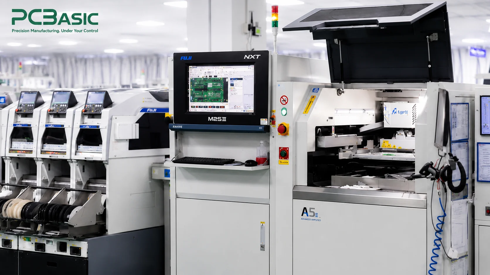
Testing helps verify that high-reliability edge computing PCBA meets specified requirements prior to release. As many of these circuits operate continuously or perform time-sensitive functions, QA goes much further than just visual examination.
The AOI rapidly identifies mistakes related to placing components, polarity problems, and problems with soldering. The X-ray system is used to inspect the solder connections that are not visible under BGA devices.
Last, functional circuit testing ensures the functionality of the edge computing PCB assembly in actual operation. Other testing methods include burn-in testing, thermal cycling, and environmental stress screening for verification of reliability.
There is a growing need for edge computing PCB assembly, especially with the rise of AI, machine learning, and Industrial Internet of Things. Edge computing makes it possible to process data close to the source, which helps minimize latency and ensure the security of data. Below is a list of some of the most common applications for AI hardware PCB assembly
They require highly efficient edge AI PCB assembly components that include an AI processor, image sensors, memory and communication modules all packed together in one tiny piece of hardware. With local processing, video cameras become able to respond instantly while using less network bandwidth and securing data.
Due to the fact that many surveillance systems operate continuously, and outdoor models may face demanding environmental conditions, the manufacturer should make sure that the high-reliability edge computing PCBA and overall product design can withstand expected temperature changes, humidity, dust, and vibration.
The IoT gateways in factories act as a communication center connecting factory machinery, sensors, cloud servers, and the enterprise network infrastructure. They gather data from different sources, perform local processing, and send it to the cloud.
The high-quality AI hardware PCB assembly may integrate communication interfaces supporting Ethernet, CAN Bus, Modbus, RS485, and wireless technologies such as Wi-Fi, Bluetooth, and 5G.
Industrial environments often provide electrical noise, temperature extremes, and permanent operation of electronics. Thus, edge computing PCBA should undergo inspection and testing based on the application and operating requirements.
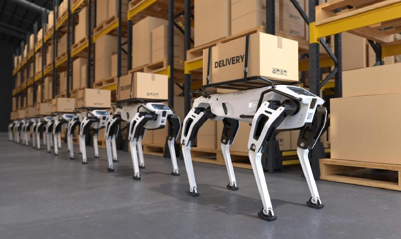
Autonomous Mobile Robots (AMRs), collaborative robots, or Cobots, and Automated Guided Vehicles (AGVs) require edge computing capabilities to navigate, detect objects, and make decisions independently.
The PCBA designs of these devices are embedded with AI that has processing components, interfaces for sensors, controllers for motor control, wireless communications, and power management in multilayer PCBs. They are designed for manufacturing and warehouse applications and require quality production and thorough testing.
In the healthcare sector, edge AI module PCBAs are being used in various applications such as medical imaging, portable diagnostics, patient monitoring, and wearable health devices. With edge AI, patients can have their data analyzed in real time while reducing the need to transmit sensitive raw data externally. In such devices, high-reliability, small size, and low-power-consumption PCBAs with good signal integrity are needed. Before use, inspection and testing may include AOI, X-ray, and FCT, depending on the design and quality requirements.
The choice of a suitable edge computing PCB assembly manufacturer is equally critical as the design process itself. The right manufacturer would help increase product reliability, shorten development time, and minimize manufacturing risks. While choosing a PCB assembly company to work with, pay attention to the following aspects:
● Manufacturing Excellence: Ensure the manufacturer provides services for manufacturing multilayer boards, HDI PCB fabrication, fine-pitch BGA assembly, and high-density SMT assembly.
● Engineered Design: Ensure the manufacturer possesses expertise in DFM and DFT to achieve better results during the production process.
● Testing Services: Pick a manufacturer offering AOI testing, X-rays, ICT, functional circuit testing, and reliability tests.
● Certifications and Compliance: Check whether the manufacturer holds relevant certifications such as ISO 9001 or ISO 13485 and follows applicable IPC standards and RoHS requirements.
● Full-Spectrum Services: The reliable manufacturer is expected to offer PCB fabrication, sourcing of components, SMT assembly, testing, and rapid prototyping in-house, thus making project management easy.
For companies creating AI-enabled devices, collaboration with a professional manufacturer like PCBasic gives the opportunity to use PCB assembly services that feature cutting-edge technology of edge computing, strict control of quality, and custom manufacturing solutions. With the help of professionals in AI hardware PCB assembly, high-density PCB fabrication, and testing services, PCBasic will assist you in turning the innovations of edge computing into the production of electronic devices.
As edge computing devices evolve towards higher computing power and more compact designs, edge computing PCB assembly needs to simultaneously address high computing density, thermal management, signal integrity, and long-term reliability. To achieve stable and reliable product performance, it not only depends on PCB design, but also requires reasonable SMT assembly processes, appropriate inspection and testing, as well as quality control throughout the production process.
The specific manufacturing plan should also be adjusted according to the actual application requirements. Whether the product is used in AI intelligent cameras, industrial IoT gateways, autonomous robots, or medical edge devices, it is necessary to comprehensively consider its working environment, performance requirements, and reliability goals. Collaborating with experienced PCBA manufacturers can help identify manufacturability issues earlier and reduce manufacturing risks from sample development to mass production. PCBasic can provide one-stop PCBA services for edge computing and AI hardware projects, including PCB manufacturing, component procurement, precise SMT assembly, inspection and testing.
Q1: What is Edge Computing PCB Assembly?
A1: Edge computing PCB Assembly is the process of assembling electronic components onto printed circuit boards used in edge computing devices. Thanks to that, such boards allow local data processing and enable AI systems to process data locally with low latency without using only cloud servers. It reduces latency, increases security and speeds up decision-making.
Q2: How is Edge Computing PCB Assembly different from standard PCB assembly?
A2: In contrast to ordinary PCB assemblies, edge computing PCBA includes the assembly of high-performance processors, AI accelerators, memory modules, and communication interfaces. Such boards require advanced thermal management, impedance routing, and reliability testing as well.
Q3: What industries use AI Hardware PCB Assembly?
A3: AI hardware PCB assembly is applied in:
● AI-powered smart cameras
● Industrial IoT gateways
● Autonomous robots and AGVs
● Medical diagnostic equipment
● Smart transportation systems
● Retail automation
● Smart agriculture
● Edge AI servers and embedded devices
These uses require real-time processing and reliable performance from the hardware.
Q4: Why is thermal management important in AI Edge Computing PCBs?
A4: Heat is generated by the AI processor when in use all the time. Thermal management through thermal vias, copper planes, heat sinks, and PCB layout design ensures the AI edge computing PCB does not overheat and is able to function reliably.
Q5: What testing methods are used for High-Reliability Edge Computing PCBA?
A5: The manufacturer carries out a variety of inspection and testing processes such as:
● Automated Optical Inspection (AOI)
● X-ray Inspection
● In-Circuit Testing (ICT)
● Functional Circuit Testing (FCT)
● Burn-in Testing
● Thermal Cycling
● Environmental Stress Screening (ESS)
These methods help verify that each high-reliability edge computing PCBA meets defined quality and functional requirements.
Assembly Enquiry
Instant Quote


Phone contact

+86-755-27218592
In addition, we've prepared a Help Center. We recommend checking it before reaching out, as your question and its answer may already be clearly explained there.
Wechat Support

In addition, we've prepared a Help Center. We recommend checking it before reaching out, as your question and its answer may already be clearly explained there.
WhatsApp Support

In addition, we've prepared a Help Center. We recommend checking it before reaching out, as your question and its answer may already be clearly explained there.
