
Global high-mix volume high-speed PCBA manufacturer
9:00 -18:00, Mon. - Fri. (GMT+8)
9:00 -12:00, Sat. (GMT+8)
(Except Chinese public holidays)





HomePage > Blog > Knowledge Base > BMS PCB Assembly Is More Than SMT: What Makes a BMS Board Reliable?
Table of Contents
1. Why BMS Reliability Cannot Be Built by SMT Alone
2. Design Choices That Become Assembly Risks
3. Production Controls That Go Beyond Component Placement
4. Inspection Finds Defects; Functional Testing Proves Protection
5. What Engineers Should Define Before Requesting a BMS PCBA Quote
6. Conclusion
7. FAQs
In light of the growing popularity of electric vehicles, energy storage systems, and industrial batteries, the global battery management system market is set to exceed $12 billion in 2026 (Grand View Research). As BMS production volumes keep growing, manufacturers cannot afford to consider BMS PCB assembly just another surface mount technology job anymore. The process is far more demanding than assembling other types of PCBs.
This article will outline the aspects that make a battery management system reliable and what distinguishes its manufacturing process from the one of a traditional SMT PCB. In addition, it will give a few pointers on the information required to request a BMS PCB assembly quote.
While the exact placement of components is vital, BMS PCBA is expected to perform functions that a regular consumer board will never have to do. A battery management system PCBA is found at the junction between the raw cell voltage and anything that needs to be protected by the pack, such as people, machines, and the battery.
Once assembled, a BMS board constantly monitors the voltage of the cell, pack current, and the temperature to ensure the safe operation of the battery. Using the information gathered, it controls the balancing circuits, contactors, and protection switches when required. Even the smallest manufacturing problem such as a poor solder joint, misaligned shunt resistor, or any contamination of a trace will affect measurement accuracy or protection response. In lithium battery systems, such errors may reduce the BMS's ability to detect or respond correctly to abnormal conditions.
The accurate state of charge (SOC) and state of health (SOH) calculations also rely on the stable operation of the sensors for the whole lifetime of the battery, rather than at the testing phase. The manufacturing problem that does not seem critical in the beginning, such as increased resistance of a sense line connection, will aggravate during further heating-cooling cycles.
High-current traces are commonly routed close to low-level signal circuits on a BMS board. Although this is a space-saving assembly layout, it increases assembly challenges. In a standard SMT assembly line, different component sizes, pad structures, and copper areas can create different thermal requirements. In the case of BMS boards, however, large copper areas are used in combination with very sensitive signal chains and conventional setup of reflow soldering might not provide expected results for the entire board.
One good example is a two-ounce copper area near a 0402 component. Their different thermal masses can create a wider process window that must be considered during reflow profiling. The reflow profile should therefore be optimized for the complete assembly so that both high-thermal-mass areas and nearby small components remain within acceptable soldering and temperature limits.

Many assembly problems can originate from the PCB design phase. Issues like copper weight, trace width, and pad sizes have a direct impact on how the board will perform in the soldering process. High power pads and heavy copper parts conduct heat in a different manner compared to small signal devices around them. Therefore, they cannot all share the same amount of solder paste.
Due to the nature of high power BMS PCB assembly, stencil design is not enough. It is important to consider the stencil design, the application of solder paste, and the reflow process in relation to the high power parts but without compromising the low power parts around them.
The shunt resistors and current sense amplifiers provide one of the most delicate measurements performed on the circuit board, and placement of these elements near high current traces has a direct bearing on their accuracy. Just a small change in orientation during placement or the solder wicking under the shunt can introduce additional resistance or measurement error.
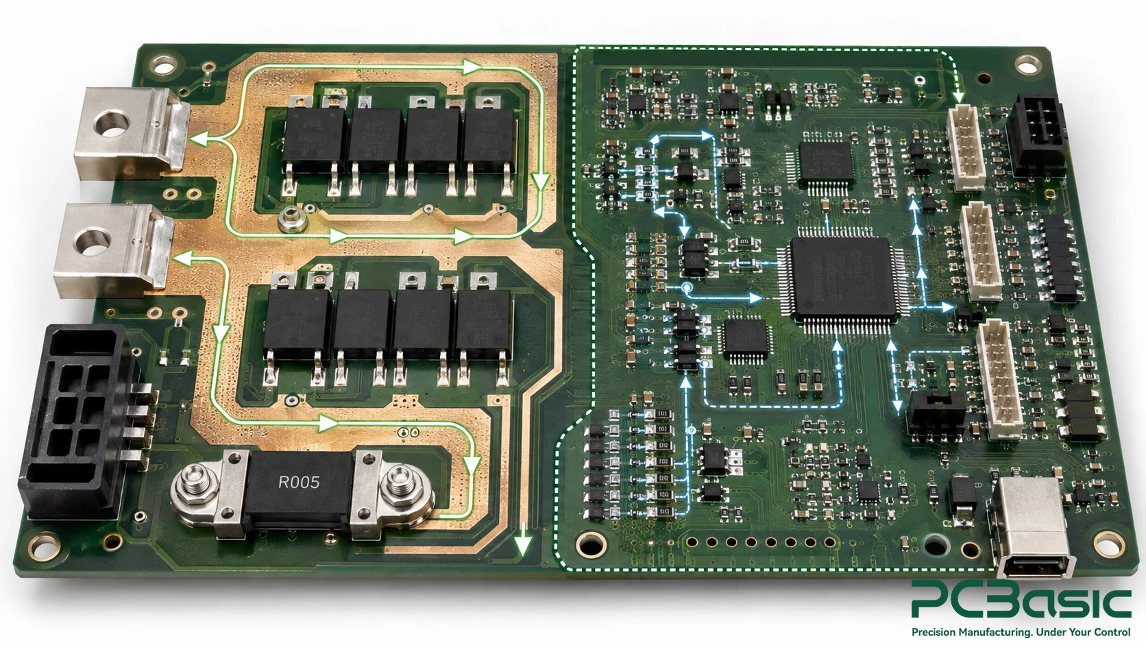
Heat produced by the power MOSFET, balancing resistors, and current sense circuitry needs to be regulated in order to make sure that the temperatures are measured accurately. In order to ensure this, engineers during BMS PCB fabrication take care of positioning copper pours and thermal vias in such a way that the heat is diverted away from the temperature sensors.
High-voltage or distributed BMS boards may use isolators or opto-couplers to separate the high voltage battery circuitry from the low voltage communication and control circuits. During assembly, it becomes important that the proper creepage and clearance values are achieved. It becomes very difficult to perform the in-circuit tests in case test points are not accessible even after the application of conformal coating.
The communication interface through CAN, UART, and isolated SPI sends the balancing commands and fault information across the isolation barrier. Even the slightest displacement near an isolator leads to lower creepage value without triggering any kind of fault. Such problems occur only during the occurrence of high voltage spikes. Due to this, isolation footprints are always checked with respect to the BMS PCB layout.
Any board that will be placed on an SMT line is first analyzed by an experienced BMS PCBA manufacturing partner who will check the bill of materials for obsolete components, inappropriate replacements, and long-lead-time components. In the design-for-manufacturing analysis, footprint misalignments, insufficient clearance, and problematic stencil aperture designs that do not provide sufficient solder paste to the power pads are identified.
Replacement of components in a BMS board requires special attention since a replacement of a precision resistor or reference will shift the tolerance stack-up sufficiently to influence the calibration of the board. The material review process identifies such potential changes so that the engineering department can decide whether it is appropriate or not.
Components like precision resistors, current sensing shunts, and isolators often require more care than what can be delivered by an ordinary SMT process. There may be cases where some of them will require special reflow profiles, selective wave soldering of through-hole connectors, and manual inspection which is difficult to validate by the automated systems. High-reliability battery management system PCBA requires validation of these vital processes rather than mere reliance on visual inspection alone. High-reliability PCB assembly begins with ensuring all of these elements.
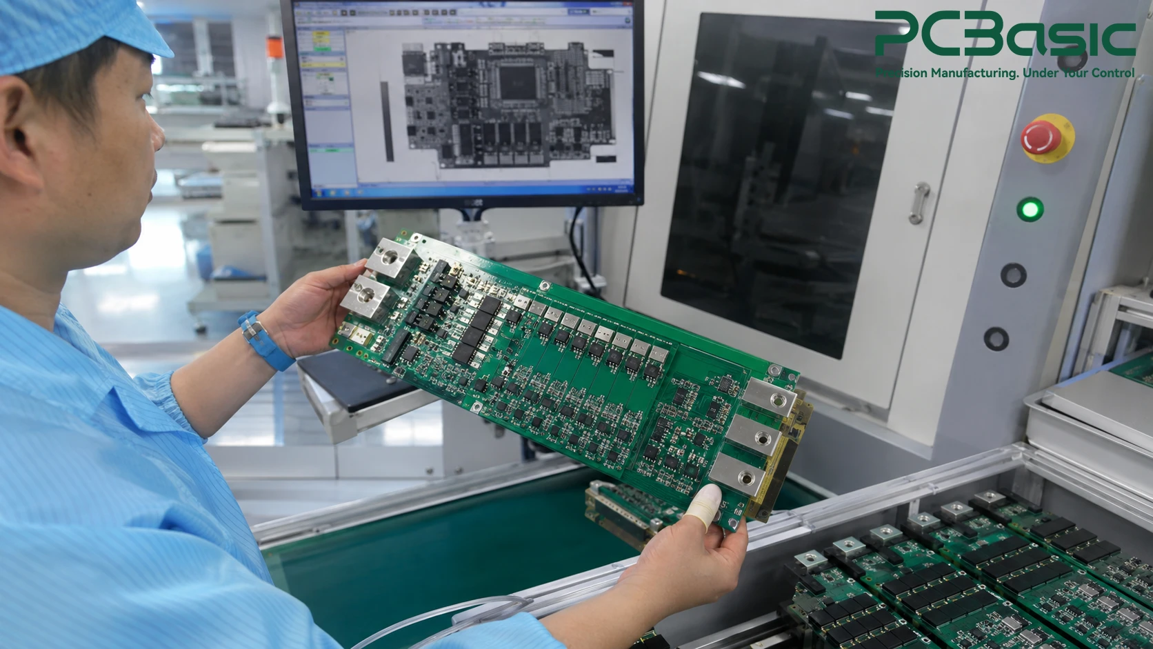
The conformal coating prevents moisture and dust from affecting the board within a real battery housing, but the conformal coating should not affect connectors, test points, or sensitive components to the chemicals in the coating. Selective coating, selective masking, and proper curing for the conformal coating type are necessary for a BMS electronics manufacturing process that focuses more on durability than speed.
Cleaning is equally important to the coating process. Even residual flux left close to the shunt resistor or a high-impedance sensing point can form leakages that affect the measurement result over an extended period of time, long after the board has been tested functionally. In some cases, even boards that use a no-clean paste should be cleaned around sensitive analog parts during energy storage PCB assembly.
Solder paste inspection, automated optical inspection, and X-ray each catch different problems, and none of them alone confirms a board will protect a battery pack correctly.
|
Inspection Method |
What It Catches |
Where It Runs |
|
SPI |
Paste volume, alignment, and bridging risk before reflow |
Right after paste printing |
|
AOI |
Missing, shifted, or wrong-polarity parts; solder bridges |
After reflow, before functional test |
|
X-Ray |
Hidden joints under QFN and BGA packages, solder voiding |
After reflow, on power and sensing ICs |
Passing through the process of inspection means only that the circuit board is okay, but it does not mean that the assembly of the battery management system circuit board functions properly. In order to check this, functional testing needs to be done using simulated cell voltage and loads.
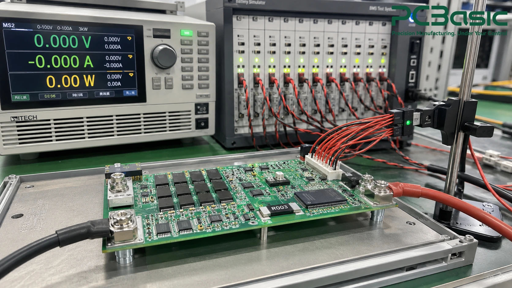
There are also certain builds that need to undergo burn-in tests, thermal cycling tests, or high-current loading tests as per their actual duty cycle during the usage of the energy storage PCBA. A new energy power module PCBA that will operate in tough conditions and even in vehicles will benefit from this additional verification process.
Factors like the number of cells, chemistry, voltage range, and the maximum continuous or peak current govern the copper weight on the board, the trace width, and component choices. A BMS PCB assembly manufacturer should know these figures early because they influence component selection, copper design, power connections, and thermal requirements, which in turn affect the assembly process.
IPC requirements for class, needs for conformal coating, and expected test coverage either through ICT or functional test, or both should be considered when putting in the quote request. The volume expectations are also important since different fixtures and tooling would be required for prototyping and production volumes.
Engineers gain a lot of information by asking directly how the potential vendor deals with mixed high-current and precision sensing segments, what unique control processes are used in manufacturing shunts and isolation parts, and how test coverage is verified before shipping. Such questions tell more about the potential of the company than the most detailed capabilities page would.
It is also useful to ask for an example of a test report of a similar build, rather than a specification sheet only. The company having the experience of manufacturing high-reliability BMS PCBAs should be able to provide inspection documents, test results, and information on how they were able to detect a defect in one previous build at the manufacturing stage.
PCBasic BMS PCB assembly process is structured in line with all of these requirements with the DFM review documented, reflow profiles controlled for power and sensing boards, and test capabilities in place even at the quoting conversation stage. For a new BMS project, you can submit your Gerber files, BOM, and test requirements for a project-specific review.
A robust BMS board is created through proper planning, controlled manufacturing, inspection, and testing. All the processes have an effect in minimizing the chances of any failure to occur when the battery pack becomes operational. A properly controlled BMS PCB assembly process gives engineers greater confidence in the board’s reliability after it leaves the factory. In the case where the technical needs are clearly stated, and a BMS PCB assembly company is considered from the onset, a robust battery management system can be realized.
Q1: What makes BMS PCB assembly different from standard PCB assembly?
A1: A BMS board needs to be able to control the power paths as well as the sensitive sensor paths, which is not something that is common on a normal PCB. Therefore, the need for tight management of solder paste application, reflow process, inspection, and testing of the board becomes important.
Q2: Why does shunt resistor placement matter so much in BMS boards?
A2: The shunt resistor will be used to measure the battery current; hence, any wrong positioning or excessive amount of soldering material on the resistor will affect the accuracy of measurement. Wrong measurements may cause unwanted protection trips or, worse still, prevent detection of any fault that exists.
Q3: What testing should a BMS PCBA go through before shipment?
A3: A quality BMS PCBA would usually go through a number of test processes. SPI is performed after solder paste printing, while AOI is typically used after component placement or reflow, and X-ray inspection can be used after soldering to check hidden joints. Functional testing is then carried out under simulated battery conditions. For critical applications, tests such as thermal cycling could also be necessary.
Q4: What information does a manufacturer need to quote a BMS PCB assembly?
A4: When all the information is provided, it allows for better quoting from the manufacturer’s side. Information like the chemistry type of batteries, number of cells, voltage and current, IPC Class, conformal coating requirement, and expected test level ensures that the assembly process can be planned properly from the very beginning.

Assembly Enquiry
Instant Quote



Phone contact

+86-755-27218592
In addition, we've prepared a Help Center. We recommend checking it before reaching out, as your question and its answer may already be clearly explained there.
Wechat Support

In addition, we've prepared a Help Center. We recommend checking it before reaching out, as your question and its answer may already be clearly explained there.
WhatsApp Support

In addition, we've prepared a Help Center. We recommend checking it before reaching out, as your question and its answer may already be clearly explained there.
