
Global high-mix volume high-speed PCBA manufacturer
9:00 -18:00, Mon. - Fri. (GMT+8)
9:00 -12:00, Sat. (GMT+8)
(Except Chinese public holidays)





HomePage > Blog > Knowledge Base > EV Charger PCB Assembly: Different Boards, Different Manufacturing Challenges
1. What Does a PCB Assembly Do Inside an EV Charger?
2. How Power Requirements Affect EV Charger PCB Assembly
3. From Fine-Pitch SMT to Power Component Assembly
4. Testing EV Charger PCB Assemblies for the Right Failure Modes
What does this have to do with manufacturing? In fact, it has a significant relationship. The requirements for EV charger PCB assembly of different circuits also vary. Control circuits may mainly use precision SMT components, while power-related circuits may involve large connectors, relays, through-hole components, as well as higher current-carrying and heat dissipation requirements. Therefore, manufacturing the EV charger PCBA is not simply mounting components on the EV charger PCB; it requires choosing appropriate assembly, soldering and testing methods based on the actual functions of the circuits.
In this article, we will start by explaining the functions of different circuits inside the EV charger, and see what practical impacts high currents, high voltages and heat will have on PCB assembly, as well as how these requirements are implemented in the production process. At the same time, we will also introduce the specific roles of SMT, through-hole power component assembly, AOI, X-Ray and functional testing in EV charger PCBA manufacturing.
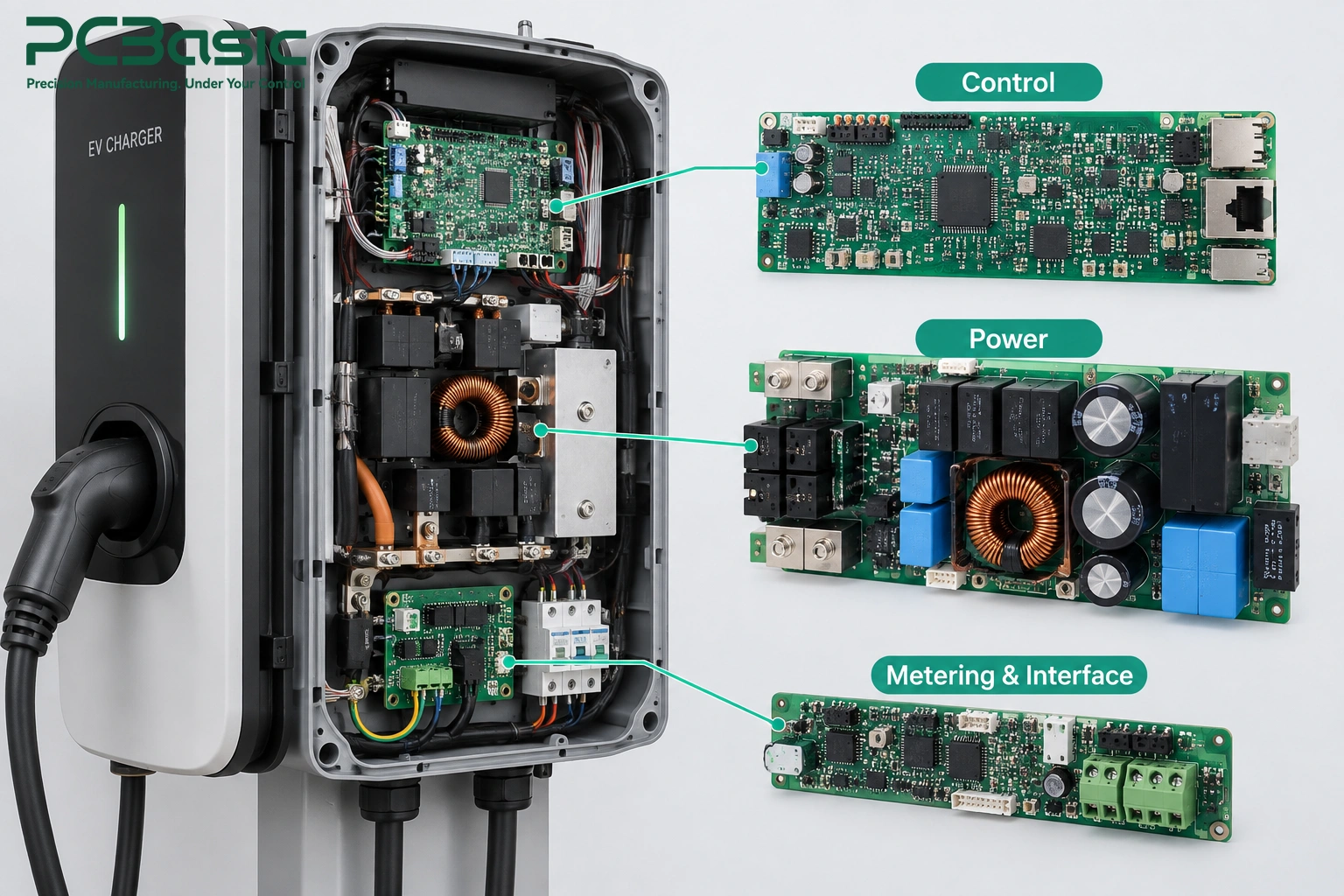
An EV charger usually has more than one type of circuit. Different PCBs perform different tasks. Depending on the specific system architecture, the EV charger PCB may be responsible for control and communication, power management, metering, protection, or it may be responsible for connecting external devices. Due to the different functions, the used components are different, and the subsequent assembly and testing requirements will naturally also be different.
|
Function |
Typical Electronic Components |
Primary Assembly Focuses |
|
Control & Communication |
MCU, communication ICs, sensing circuit |
SMT accuracy, programming, functional testing |
|
Power & High-Current |
Power devices, relays, drivers, large connectors |
Current handling, thermal load, solder joint quality |
|
Metering & Interfaces |
Metering IC, Connectors, I/O Circuit |
Mixed Assembly, Connector Reliability, Function Testing |
Let's take a simple example. The smart EV charger PCBA usually needs to handle charging control, network communication and status monitoring. Therefore, it may use an MCU, communication ICs, sensing circuits and a large number of SMD components. For such circuits, we pay more attention to the assembly accuracy, soldering quality, as well as whether the required functions are normal.
What about the power-related circuits? The focus is quite different. These circuits may use power semiconductors, relays, drivers and large connectors, which need to withstand greater current and higher thermal loads. Compared to small SMD components, the problems faced when mounting and soldering these devices are also different. The metering and interface parts mainly handle the connection of sensors, displays, communication ports and other external devices, and have corresponding requirements for connector installation and function testing.
So, we cannot treat all the EV charging station PCBA as the same type of circuit board for production. First, figure out what this board is responsible for, and then decide how to assemble, how to solder, which positions to check and which functions to test. For EV charger PCB assembly, this is also an important step in determining the manufacturing process.
Power-related circuits are a part that requires particular attention in EV charger PCB assembly. The reason is simple: the greater the current, the more attention needs to be paid to the current that the PCB has to carry and the heat it generates; when the voltage increases, the isolation requirements between different electrical areas become even more important. Although these issues need to be addressed in the PCB design stage first, they will ultimately affect the actual assembly, soldering, and testing.
How does high current affect PCB assembly? First, let's look at the PCB itself. For some high-current paths, an EV charger PCB may use a wider copper area, a thicker copper layer, or other current-carrying structures. A heavy copper PCB can be used to carry larger currents and also helps with heat conduction, but as the copper increases, the soldering conditions during production will also change.
We need to consider a very practical issue during soldering: a large area of copper needs to absorb and transfer more heat to reach the proper soldering temperature and form a good solder joint. Therefore, in heavy copper PCB assembly, we need to set and verify the soldering temperature curve based on the copper thickness, copper area, and the actual component configuration to ensure that the solder joints are fully wetted while avoiding excessive thermal stress on small or temperature-sensitive components.
Of course, this does not mean that all EV charger PCB need to use heavy copper. The working current of control and communication circuits may not be high, while the current-carrying requirements of power-related circuits may be completely different. Whether to use heavy copper ultimately depends on the specific electrical design.
The problems brought by high voltage are different from those caused by large currents. For high voltage PCB assembly, the creepage distance, clearance, and isolation areas are usually determined during the design stage, but during the production process, we still need to ensure that these designs will not be affected by assembly or rework.
In actual production, several key points need to be paid attention to:
• Creepage and clearance: Components, solder, or hardware cannot occupy the originally reserved safety spacing.
• Slots and isolation areas: During assembly and rework, the already designed isolation features built into the PCB should not be damaged or interfaced.
• Components and alternative parts: It is important to check not only the electrical specifications but also the package dimensions and insulation requirements.
• Soldering and rework: Attention should be paid to solder, residues, and the impact of the rework process near the isolation area.
So, we need to verify these critical areas through DFM and pre-production review before formally putting the EV charger PCBA into production. Which positions cannot be occupied? Which areas need additional inspection? These questions should be clarified before starting production.

Let's take a look at the components themselves. Power electronics PCB assembly usually involves not only small SMD components, but also may include:
• Power semiconductors
• Relays and large connectors
• Inductors and transformers
• Small resistors, capacitors, and control ICs
These components vary greatly in size and thermal characteristics, and cannot be soldered in the same way naturally. Large components and large copper areas require more heat, while small components heat up fast and cannot take a lot of heat for a long time.
This is why a power PCB may need several assembly and soldering processes. We may use a combination of SMT, through-hole assembly, reflow soldering and selective soldering to separate the different kinds of components, depending on what the actual board design is.
In an EV charger PCB assembly, there are often not just small SMD components. The control and communication area may be dominated by SMT components, while the power area may feature relays, large connectors, inductors, transformers, and other larger components. The different types of components require different assembly methods.
During production, we usually handle them separately:
• SMT components: MCU, communication ICs, resistors, capacitors, etc., will undergo solder paste printing, SPI, automatic placement, reflow soldering, and AOI inspection.
• Through-hole and power components: relays, large connectors, inductors, transformers, etc., with pins, can be assembled using through-hole technology, and then choose between wave soldering or selective soldering based on the PCB structure.
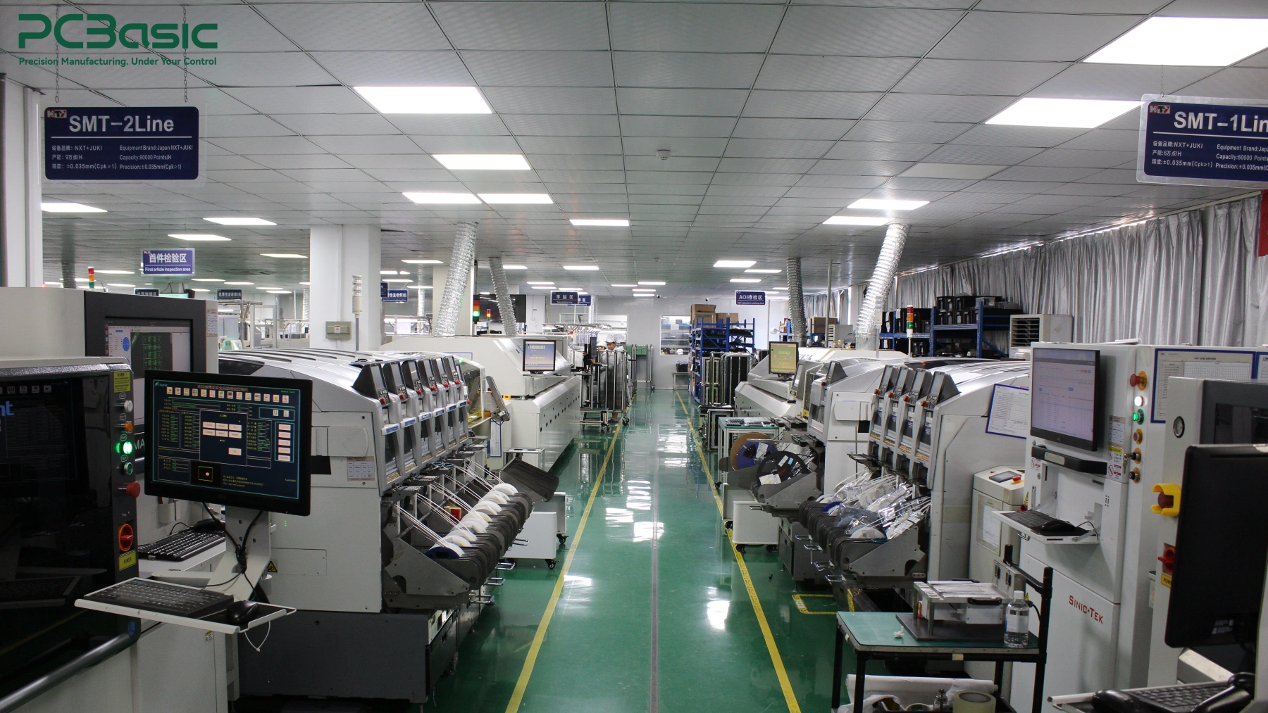
Why can't everything be assembled in the same way? Because an EV charging station PCB assembly may undergo both SMT and THT processes, and large power components, large copper areas, and small SMD components have different heat conditions. We need to arrange the assembly sequence and soldering processes according to the actual PCB.
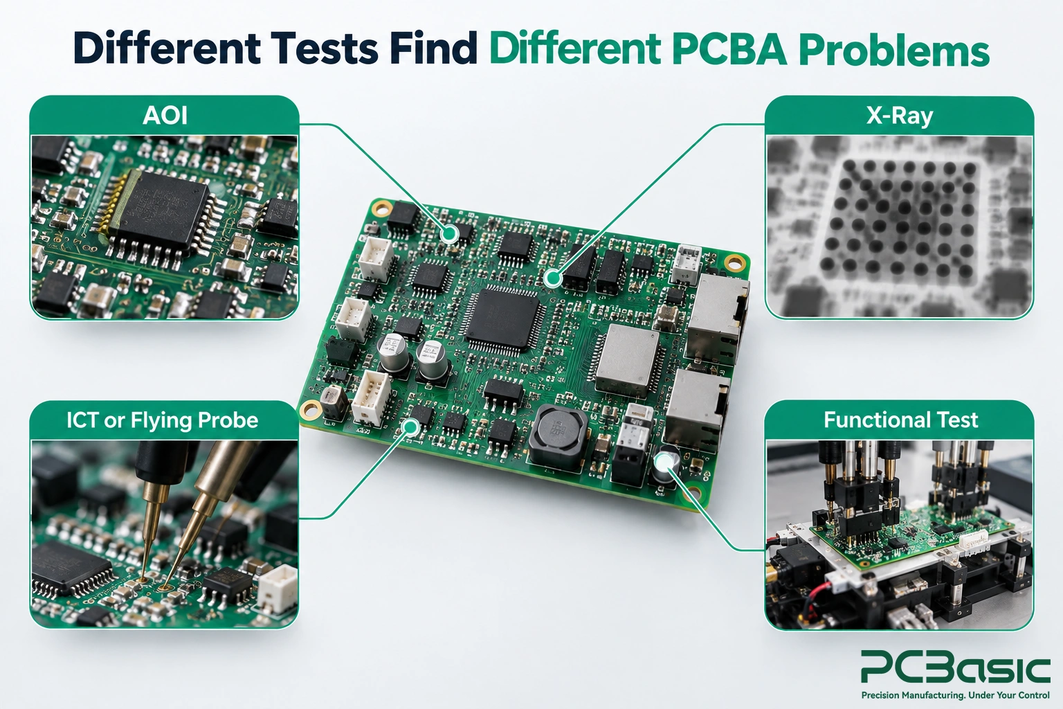
Inspection is the same. SPI and AOI can detect many problems in SMT production, but some solder joints are invisible. For example, BGA, QFN, and component with bottom thermal pads, we need to use X-Ray to further check the hidden solder joints.
At PCBasic, we arrange the production process based on the actual structure of the EV charger PCBA. SMT, DIP, wave soldering, and selective soldering can be combined according to the type of components, and are combined with SPI, AOI, and 3D X-Ray inspection instead of applying the same production process to all projects.
The AOI inspection has been passed. Does this mean the board has completed the testing? No. The AOI can detect issues such as component offset, polarity, and some soldering problems, but it cannot tell us whether the circuit can actually work properly. For EV charger PCB assembly, different problems require different inspection and testing methods.
During production, we usually combine several methods:
• SPI, AOI and X-Ray: SPI is used to check solder paste before reflow, AOI is used to detect visible placement and soldering issues, and X-Ray is employed to examine the solder joints that cannot be seen beneath BGA, QFN, etc. components.
• ICT or flying probe testing: This can check for open circuits, short circuits, electrical connections, selected component values, and circuit conditions.
• Functional testing: FCT focuses more on whether this EV charger PCBA can operate according to the design requirements. Depending on the project, we can test power-on, voltage, communication interfaces, I/O, control signals, firmware programming, and other specified functions.
So, are all the boards tested with the same set of tests? No. The issues that need attention for smart EV charger PCBA focused on control and communication, and the EV charger PCB related to power, are not the same. If the project has requirements, high-voltage or power-related PCBA may also need to undergo insulation, load or temperature rise testing.
Therefore, the test plan should be clearly confirmed before production. What needs to be tested for the EV charger station PCBA? What fixtures are needed? What firmware is required? What are the qualification standards? The earlier these pieces of information are determined, the easier it will be to maintain consistency in volume production tests. As for the safety and compliance certifications of the entire product, they need to be separated from the tests conducted during the PCBA production stage.
In PCBasic, the test plan is confirmed together during the project introduction stage. Based on the actual requirements of the EV charger PCB assembly, FAI, flying probe testing, ICT, FCT or dedicated functional test fixtures can be selected. Production and test data can also be recorded through MES, facilitating traceability during volume production.

Completing an EV charger PCB assembly is not merely about attaching components and performing soldering. We also need to consider the actual functions that this circuit board is supposed to perform. The control circuit, power circuit, high current path, and high voltage isolation area each have different manufacturing requirements, so the assembly and testing methods also need to be adjusted accordingly.
Before the EV charger PCBA enters production, we need to confirm the PCB structure, component configuration, assembly process, and testing requirements in advance. Clearly defining these requirements in the early stage can reduce rework and adjustments during production and also facilitate a smoother transition from prototype builds to mass production for the project.
If you are preparing an EV charger PCB project, PCBasic can assist in reviewing your PCB files, BOM, assembly and testing requirements before production, and develop corresponding manufacturing plans based on the actual project needs.
Q1: What is the difference between an EV charger PCB and an EV charger PCBA?
An EV charger PCB is the bare circuit board, while an EV charger PCBA is the completed board with components mounted and soldered. EV charger PCB assembly is the process of assembling those components onto the PCB.
Q2: Does every EV charger PCB require heavy copper?
No. A heavy copper PCB is mainly used when higher current-carrying capacity is required. Control and communication boards may not need heavy copper.
Q3: Why are both SMT and THT used in EV charger PCB assembly?
SMT is commonly used for small, high-density components, while THT is suitable for larger components such as relays and connectors. Many EV charger PCB assembly projects therefore use both processes.
Assembly Enquiry
Instant Quote
Phone contact

+86-755-27218592
In addition, we've prepared a Help Center. We recommend checking it before reaching out, as your question and its answer may already be clearly explained there.
Wechat Support

In addition, we've prepared a Help Center. We recommend checking it before reaching out, as your question and its answer may already be clearly explained there.
WhatsApp Support

In addition, we've prepared a Help Center. We recommend checking it before reaching out, as your question and its answer may already be clearly explained there.
