
Global high-mix volume high-speed PCBA manufacturer
9:00 -18:00, Mon. - Fri. (GMT+8)
9:00 -12:00, Sat. (GMT+8)
(Except Chinese public holidays)





HomePage > Blog > Knowledge Base > AI Server PCB: Key Requirements for Assembly and Testing
1. An Overview of AI Server PCBs and Their Types
2. PCB Requirements That Affect Assembly
3. Key Steps in AI Server PCB Assembly
4. Testing AI Server PCBAs Before System Integration
5. Why Choose PCBasic as Your AI Server PCB Assembly Partner
Unlike standard enterprise hardware, an AI server motherboard may operate under extreme thermal stress, very high signaling rates (such as PCIe 5.0/6.0 and 112G PAM4 SerDes, depending on the platform), and demanding current density requirements. For hardware engineers, component sourcing specialists, and procurement teams, sourcing an AI server PCB assembly isn't just about finding a contract manufacturer who can solder components. It requires deep technical alignment across signal integrity (SI), power distribution networks (PDN), specialized PCB fabrication, and stringent test coverage.
In this comprehensive guide, we will unpack the manufacturing, assembly, and testing requirements needed to deliver reliable AI server PCB assemblies that meet the demands of modern cloud infrastructure.
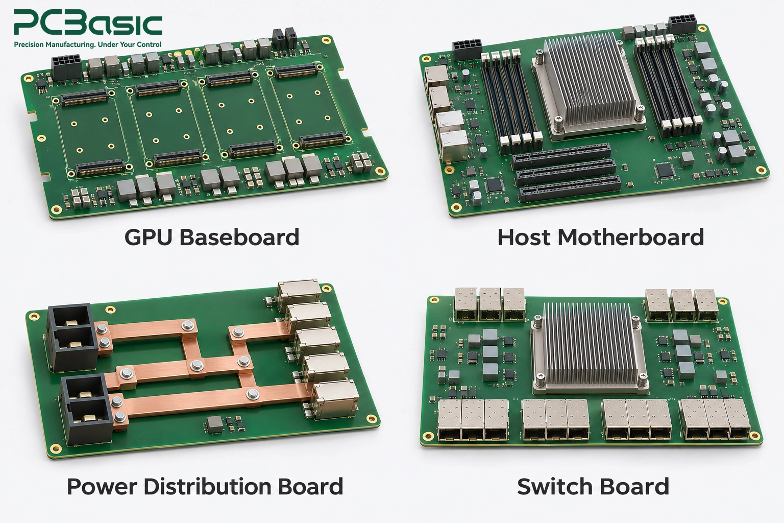
To handle the immense parallel processing power required by machine learning clusters, modern server architectures rely on specialized board configurations. Depending on where the board sits within the hardware rack, its design priorities shift between ultra-high-speed routing, high power delivery, and thermal dissipation.
These boards carry AI processor packages or accelerator modules—such as those based on GPUs, TPUs, or custom ASICs—with HBM typically integrated within the processor package where used. They feature high routing densities, potentially utilizing 20 to 30+ layers, advanced High-Density Interconnect (HDI) structures, and microvia technology to support dense signal routing, depending on the board design.
The host system board functions as the primary AI server motherboard, hosting the CPUs, system RAM, system management controllers, and storage buses. While it carries high-speed PCIe lanes connecting to the accelerator baseboards, its key challenges lie in handling extensive power distribution architectures alongside long-trace signal integrity across a large physical form factor.
Dedicated power boards and high-speed PCIe/CXL switch cards distribute power to server subsystems and handle high-speed interconnect switching within supported server architectures, respectively.
Board
Type
Typical
Layer Count
Primary
Material Focus
Key
Technical Challenge
GPU Baseboard / Accelerator
20 – 32+ Layers (HDI)
Ultra-Low Loss (e.g., selected Megtron 7
grades)
BGA Routing Density, Microvia Reliability
Host System Board
16 – 24 Layers
Very Low / Ultra-Low Loss
High-Speed PCIe 5.0/6.0 Traces, Power Planes
Switch & Expansion Card
14 – 20 Layers
Low Loss
Signal Reflection, Channel Insertion Loss
Manufacturing high-layer boards with tight tolerances introduces strict requirements that directly impact manufacturing yields during surface-mount technology (SMT) operations.
Substrates such as Panasonic Megtron 7, Tachyon 100G, or selected Rogers laminates offer low dielectric loss and dielectric constant (Dk) characteristics. However, these specialized laminates exhibit different glass transition temperatures (Tg) and coefficients of thermal expansion (CTE) compared to conventional FR-4. During SMT reflow, thermal expansion differences and uneven heating can cause PCB and package warpage, leading to defective BGA soldering such as head-in-pillow (HiP) defects or non-wetting opens.
Routing thousands of lines out of fine-pitch (0.8 mm or 0.6 mm) BGA packages may require multi-step sequential lamination HDI processes. Where via-in-pad structures are used, filled and capped vias must provide smooth, planar surfaces for soldering. Excessive residual surface irregularity on the BGA solder pad can compromise solder paste deposition during assembly.
Handling hundreds of amperes may require thicker copper power planes or multiple power layers, depending on the power distribution design. Heavy copper acts as a heat sink during the soldering process, drawing heat away from adjacent SMT pads. To prevent insufficient solder reflow, SMT engineers must tailor the thermal profiles of reflow ovens and utilize thermal relief connections where electrical and thermal requirements permit.

Achieving low defect rates in AI server PCB assembly requires tight process control at every step of the SMT and post-SMT process. Because an assembled board populated with high-end GPUs, custom heat sinks, and dense power stages represents significant financial value, process reliability is non-negotiable.
The process begins with laser-cut electro-polished stencils designed specifically for fine-pitch BGA arrays. 100% 3D Solder Paste Inspection (SPI) is recommended for critical, high-density assemblies and may be required by customer specifications. SPI measures solder paste volume, height, area, and positional offset, catching volume anomalies before components are placed.
Advanced surface mount pick-and-place equipment uses optical vision systems to position components—ranging from 0201 passives to large BGA packages—with placement accuracies matched to the package and process requirements.
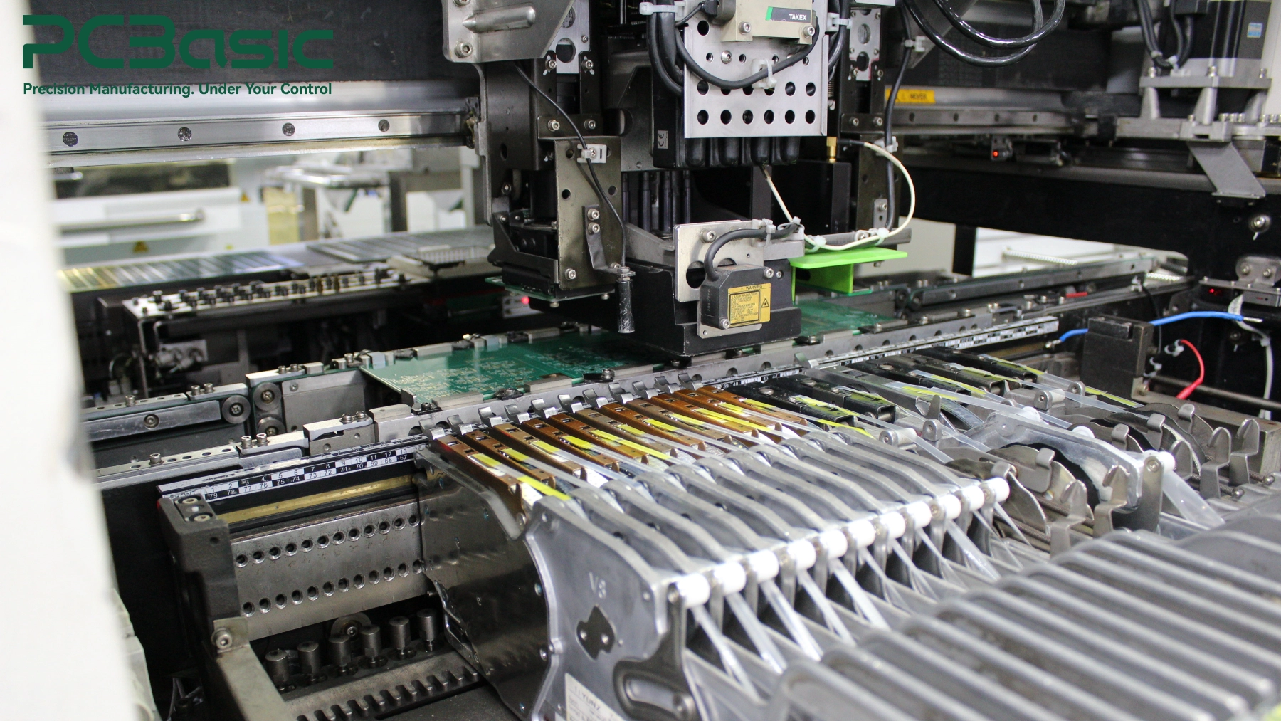
Reflow may take place in multi-zone convection reflow ovens under a nitrogen (N2) atmosphere (with residual oxygen levels defined by the validated process). Nitrogen minimizes further oxidation, improves solder wetting, and supports solder joint formation under controlled reflow conditions. Reflow profiles are tuned to limit temperature differences that can contribute to dynamic board bow and twist.
Some modern server backplanes and motherboards use heavy-duty press-fit connectors for power supplies and high-speed expansion risers. Force-monitored press-fit machines monitor insertion force in real time to reduce the risk of plated-through-hole damage or board cracking, while applicable through-hole components undergo automated selective soldering.
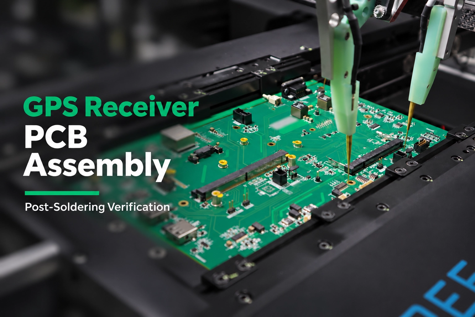
Given the structural complexity of a completed AI server PCBA, post-assembly validation must go far beyond basic visual inspection. Comprehensive multi-stage testing helps identify electrical, mechanical, and signal integrity flaws before boards are integrated into rack chassis.
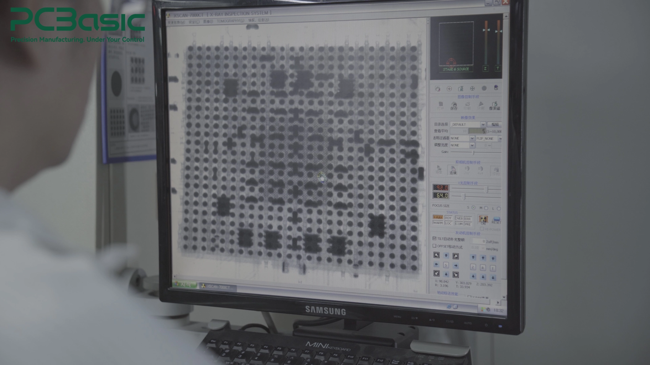
Because BGA devices have numerous hidden solder joints beneath the package, X-ray inspection is valuable for assessing solder joint quality. X-ray inspection can detect internal voids, solder bridging, and certain solder joint abnormalities beneath large chips.
ICT uses custom test fixtures to verify circuit continuity, component values, and selected electrical characteristics, helping detect shorts and opens on accessible nets. For lower-volume prototype runs, flying probe testers provide flexible coverage without requiring expensive mechanical fixtures.
High-layer-count server boards often lack physical space for test points on dense, high-speed traces. Boundary scan (IEEE 1149.1/1149.6) tests supported interconnects directly through the test circuitry of on-board ICs, checking for structural faults on compatible interfaces without directly probing each signal net. It does not replace at-speed functional testing or signal integrity validation.
Before final sign-off, boards undergo rigorous PCBA functional testing under defined operating conditions:
• Functional Testing: Functional tests verify power sequencing, firmware boot, memory operation, and communication interfaces, with load testing performed where required.
• Signal Integrity (SI) TDR Testing: Time-Domain Reflectometry (TDR) checks differential impedance along accessible high-speed traces or representative test coupons during validation.
• Thermal Stress Burn-In: Boards are operated at controlled elevated temperatures and defined electrical loads to help screen for potential infant mortality failures in power delivery components. Temperature cycling is a separate reliability test and is performed when specified by the qualification plan.

Finding a manufacturing partner capable of executing complex server PCB assembly requires balancing fabrication capabilities with rigorous quality control. PCBasic provides specialized end-to-end manufacturing services for projects with confirmed fabrication, assembly, and testing requirements.
• Advanced High-Layer Capabilities: Support for fabricating and assembling multilayer boards, with layer counts, low-loss materials, and HDI structures confirmed during engineering review.
• Strict Quality & Process Control: Inspection against agreed IPC-A-610 Class 3 acceptance criteria where specified, supported by SPI, X-ray inspection, and project-specific functional testing.
• Traceability & Component Sourcing: Robust supply chain networks supporting component authenticity verification, backed by lot-level traceability according to project requirements for sensitive ICs and power modules.
• DFM/DFA Engineering Assistance: In-house technical reviews before production runs to identify routing and thermal-design concerns and optimize stencil designs—supporting consistent yields from prototype to volume production.
As a PCB assembly partner, PCBasic bridges the gap between complex hardware design concepts and scalable, process-controlled manufacturing execution.
Building reliable high-performance server hardware requires harmonizing substrate selection, stackup design, precise assembly engineering, and comprehensive test validation. As bus speeds push deeper into multi-gigahertz ranges and board densities continue to rise, close collaboration between design engineers, procurement specialists, and your manufacturing partner is essential. By prioritizing DFM principles and rigorous testing protocols early in the design cycle, hardware teams can maximize manufacturing yields, ensure long-term field reliability, and accelerate their product rollouts.
Q1: What substrate materials are best suited for an AI server PCB?
Selected grades from high-speed laminate families, such as Panasonic Megtron 6/Megtron 7 or Isola Tachyon, may be suitable, depending on the channel loss budget and fabrication requirements. These materials feature controlled dielectric properties and low dielectric loss, with Dk and Df values depending on the specific grade, construction, and test conditions, which help limit signal attenuation in high-speed channels.
Q2: Why is X-Ray inspection useful for an AI server motherboard assembly?
Large BGA and certain surface-mount socket packages feature numerous solder contacts completely hidden from optical cameras. X-Ray inspection examines these hidden solder joints, identifying voiding, bridging, and certain open-joint defects, depending on inspection capability, without damaging the assembly.
Q3: How do assembly teams manage warpage on large, high-layer server PCBs?
Warpage is managed through balanced stackup design during fabrication, suitable substrate selection, tailored SMT reflow temperature profiling, and the use of appropriately designed SMT support fixtures where needed to help control board deformation during heating cycles.

Assembly Enquiry
Instant Quote



Phone contact

+86-755-27218592
In addition, we've prepared a Help Center. We recommend checking it before reaching out, as your question and its answer may already be clearly explained there.
Wechat Support

In addition, we've prepared a Help Center. We recommend checking it before reaching out, as your question and its answer may already be clearly explained there.
WhatsApp Support

In addition, we've prepared a Help Center. We recommend checking it before reaching out, as your question and its answer may already be clearly explained there.
