
Global high-mix volume high-speed PCBA manufacturer
9:00 -18:00, Mon. - Fri. (GMT+8)
9:00 -12:00, Sat. (GMT+8)
(Except Chinese public holidays)





HomePage > Blog > Knowledge Base > Smart Socket PCB Assembly: How Smart Sockets Are Built and Tested
1. What Does a Smart Socket PCBA Do?
2. Key Components Inside a Smart Socket PCBA
3. Common Challenges in Smart Socket PCB Assembly
4. The Smart Socket PCB Assembly Process
5. How Smart Socket PCBAs Are Tested
Whether you are scaling up pilot production or refining an existing design, understanding the nuances of smart socket PCBA manufacturing helps you avoid costly redesigns, regulatory compliance failures, and field reliability issues. In this guide, we will break down what goes into a high-performance smart socket circuit board, explore the intricacies of the smart socket PCB assembly process, and look at how rigorous smart socket PCBA testing protects your brand reputation.
A smart socket is much more than a mechanical relay enclosed in plastic; it is a compact edge-computing and power-switching node. The smart socket control board acts as the central nervous system of the device, executing several critical functions simultaneously:
1. Power Management and Conversion: It converts mains AC power at the product’s rated input voltage to low DC voltages (usually 3.3V or 5V) to power the microcontroller and wireless communication modules.
2. Wireless Connectivity: In Wi-Fi models, through a dedicated Wi-Fi subsystem or integrated module, it connects to local home routers, enabling cloud communication, remote smartphone app control, and supported smart home platform integrations, depending on the firmware and ecosystem requirements.
3. Load Switching: Using electromechanical relays or solid-state switches, it controls the AC power supplied to the appliance plugged into the socket.
4. Energy Monitoring and Safety Protection: Advanced boards integrate metering ICs to track parameters such as voltage, current, power factor, and cumulative energy consumption, alongside separate overcurrent, overvoltage, and overtemperature protection feature where provided by the design.
To build a robust smart socket PCB, selection and placement of components require careful attention to electrical ratings, thermal limits, and physical dimensions. The typical bill of materials (BOM) includes:
• Microcontroller Unit (MCU) / Wi-Fi SoC: Systems-on-Chip (SoCs) such as the ESP8266, ESP32, or selected Realtek and Nordic devices are possible choices because they combine processing power with wireless connectivity, although supported protocols vary by device. The ESP8266 supports Wi-Fi, while the ESP32-C3 supports both Wi-Fi and Bluetooth LE.
• Power Supply Unit (PSU): Typically a miniature AC-DC switching power supply module or a discrete circuit utilizing a switching regulator, filtering capacitors, and, in isolated flyback designs, a transformer to deliver stable DC power. A low DC output voltage does not necessarily indicate electrical isolation from the mains.
• Electromechanical Relays or Triacs: The heavy-lifters of the board. Relays must be rated for high inrush currents (especially for inductive loads like motors or compressors) and continuous current ratings (e.g., 10A, 13A, or 16A).
• Energy Metering ICs: Chips like the HLW8012 or BL0937 measure voltage and current parameters accurately, feeding data back to the MCU.
• Passive Components: Resistors, ceramic and electrolytic capacitors, and inductors for decoupling, noise filtering, and impedance matching.
• Connectors and Terminals: Screw terminals, spring-cage connectors, or copper busbars that handle the high-current AC input and output paths.
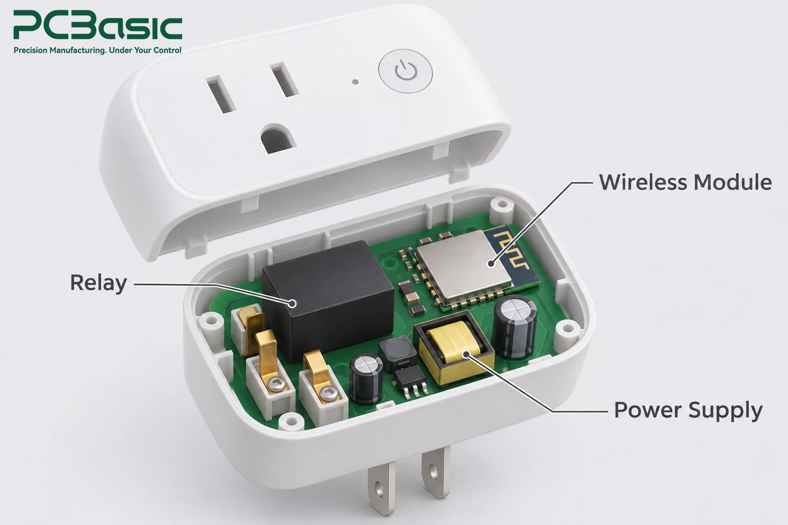
Designing and assembling a smart socket introduces unique engineering challenges that differentiate it from standard low-voltage consumer electronics.
Because these boards handle mains voltage, applicable product safety standards specify minimum creepage and clearance distances between conductive parts that require insulation separation. These distances depend on working voltage, insulation type, pollution degree, material group, and altitude. Failing to maintain adequate creepage and clearance on the smart socket PCB layout can lead to arcing, electrical shock, or short circuits during certification testing.
Relays and switching power supplies generate localized heat. If traces are too narrow or component placement is too dense, thermal buildup can degrade electrolytic capacitors, cause sensor readings to drift, or contribute to premature solder joint fatigue.
Carrying 10 to 16 Amps of current may require wide copper traces, heavier copper, or even auxiliary copper busbars soldered directly onto the smart socket circuit board to limit excessive I2 R heating and voltage drop, depending on the board construction and allowable temperature rise.
Switching power supplies and wireless radios operating on the same compact smart socket PCBA can create severe EMI. Proper grounding, shielding where needed, and careful routing of RF feedlines and placement of antennas are important for meeting applicable EMC and radio requirements in target markets.

Executing a seamless smart socket PCB assembly process requires a disciplined, high-precision manufacturing flow, often combining surface mount technology (SMT) with through-hole technology (THT) due to the presence of components such as mechanical relays and terminal blocks.
1. Solder Paste Printing and Inspection (SPI): High-precision stencil printers deposit lead-free solder paste onto the bare smart socket PCB. Automated SPI systems inspect paste volume and alignment to prevent bridging or insufficient solder joints.
2. SMT Placement: Pick-and-place machines mount surface-mount components—such as MCUs, resistors, ICs, and small passive parts—at high speeds onto the paste-coated pads.
3. Reflow Soldering: The populated boards pass through a multi-zone convection reflow oven with a carefully profiled thermal curve, ensuring reliable intermetallic bonding without overheating sensitive semiconductor packages.
4. Automated Optical Inspection (AOI) / X-Ray Inspection: AOI checks for missing parts, skew, and tombstoning. X-ray inspection may be used to inspect hidden solder joints underneath bottom-terminated components (like QFN packages or certain power modules), depending on the inspection plan.
5. Through-Hole Insertion and Wave/Selective Soldering: Heavy components like relays, large transformers, and terminal blocks are inserted either manually or via automated insertion machines. Because smart sockets may feature a mix of surface-mount ICs and thermal-mass through-hole pins, selective soldering can be used to form controlled solder joints while limiting heat exposure to adjacent components.
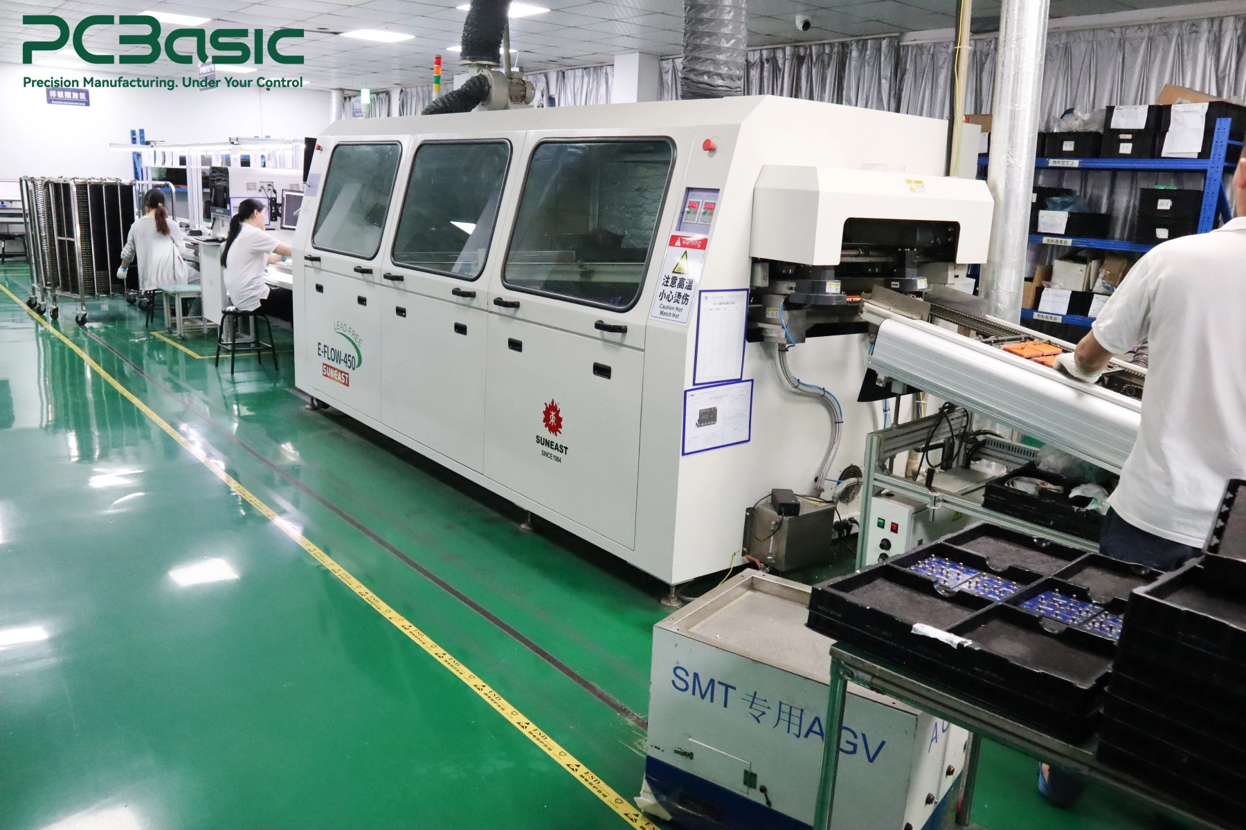
6. Conformal Coating (Optional): For use in humid or dusty environments, a protective polymer coating may be applied to the smart socket control board to reduce the effects of moisture, condensation, and contamination. Conformal coating does not replace appropriate enclosure protection or required insulation measures.
At PCBasic, SMT and through-hole assembly are supported by solder paste inspection, AOI, and X-ray inspection where required. MES traceability helps link production records to each batch, making it easier to investigate process issues and manage repeat orders.
Quality assurance is the final defense against field failures, safety hazards, and costly product recalls. A comprehensive smart socket PCBA testing strategy typically encompasses multiple tiers of evaluation.
For smart socket projects, PCBasic can work with customers to define board-level test coverage based on the circuit design and product requirements. Available testing capabilities include flying probe, ICT, and FCT, with test access and fixture requirements reviewed before production.
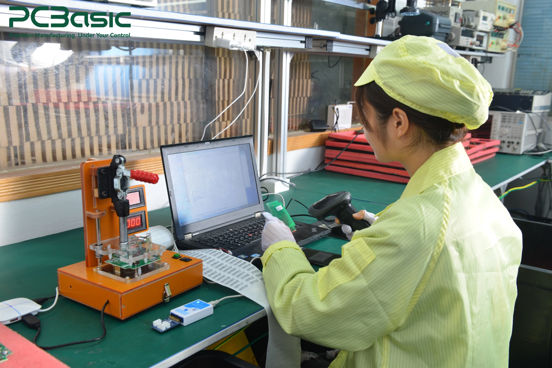
• In-Circuit Testing (ICT): Checks for short circuits, open circuits, component values, and basic diode/transistor characteristics on the assembled PCB before functional power-up, subject to test access and circuit constraints.
• Automated Functional Testing (FCT): A custom test jig powers up the Wi-Fi smart socket PCBA, flashes the firmware where required, verifies Wi-Fi pairing capabilities, tests relay switching under specified load conditions, and calibrates the energy-metering function where fitted to meet the specified measurement accuracy.
• High-Potential (Hi-Pot) Testing / Dielectric Withstanding Test: Required where specified by the applicable product safety standard. This test applies a specified high voltage across the relevant insulation barriers to verify insulation integrity, using test points, voltage, duration, and leakage-current limits defined in the approved test procedure.
• Burn-In and Environmental Stress Testing: Samples from production batches may undergo specified temperature, load, and power-cycling tests to identify early-life component failures, according to the reliability test plan.

Successfully bringing a connected power device to market requires more than just a clever circuit diagram—it demands meticulous attention to layout rules, stringent safety standards, and a robust manufacturing partner. Mastering every stage of smart socket PCB assembly, from component selection to advanced smart socket PCBA testing, helps your product stand out in a crowded market for its reliability, safety, and performance.
PCBasic provides PCB fabrication, component sourcing, assembly, and testing support for prototype and production orders. Share your Gerber files, BOM, and test requirements with our team to discuss manufacturability, inspection coverage, and quotation options for your smart socket project.
Q1: What PCB material thickness and copper weight are recommended for smart sockets?
For 10 A to 16 A smart sockets, FR-4 material with a thickness of 1.6 mm is a common starting point, subject to mechanical and safety requirements. However, using heavier copper, such as 2 oz instead of 1 oz, may be appropriate for high-current power paths to reduce resistive heating and voltage drop, depending on conductor width and allowable temperature rise.
Q2: Why are clearance and creepage distances critical in smart socket PCB design?
Clearance (distance through air) and creepage (distance along an insulating surface) help prevent insulation breakdown between conductive parts that require insulation separation. Meeting the applicable minimum distances is necessary for compliance with relevant product safety standards.
Q3: What is the difference between SMT and THT in smart socket assembly?
Surface Mount Technology (SMT) is used for smaller, lightweight components like MCUs, passive resistors, and chips. Through-hole technology (THT) is commonly used for bulky, mechanical, or high-current components—such as through-hole relays, terminal blocks, and transformers—that require strong physical anchoring to withstand mechanical stress.
Q4: How can procurement teams ensure quality during smart socket PCBA manufacturing?
Procurement teams should verify that the contract manufacturer (CM) holds relevant quality management certifications (e.g., ISO 9001), implements rigorous incoming material inspection (IQC), utilizes AOI and X-ray inspection as appropriate, and performs functional testing and any required routine electrical safety testing according to the agreed quality plan before shipping.

Assembly Enquiry
Instant Quote

Phone contact

+86-755-27218592
In addition, we've prepared a Help Center. We recommend checking it before reaching out, as your question and its answer may already be clearly explained there.
Wechat Support

In addition, we've prepared a Help Center. We recommend checking it before reaching out, as your question and its answer may already be clearly explained there.
WhatsApp Support

In addition, we've prepared a Help Center. We recommend checking it before reaching out, as your question and its answer may already be clearly explained there.
