Global high-mix volume high-speed PCBA manufacturer
9:00 -18:00, Mon. - Fri. (GMT+8)
9:00 -12:00, Sat. (GMT+8)
(Except Chinese public holidays)
Global high-mix volume high-speed PCBA manufacturer
9:00 -18:00, Mon. - Fri. (GMT+8)
9:00 -12:00, Sat. (GMT+8)
(Except Chinese public holidays)
HomePage > Blog > Knowledge Base > SOIC Package – Small Outline Integrated Circuit
The Small Outline Integrated Circuit (SOIC) package is one of the most popular and widely used surface mount package types in integrated circuits. With electronics transitioning to smaller sizes and higher component density on printed circuit boards, SOIC packaging has become one of the enabling technologies.
In this article, we’ll tell you more about the SOIC package, its main features, benefits, use cases, typical modifications, and comparisons with other types of IC packaging.

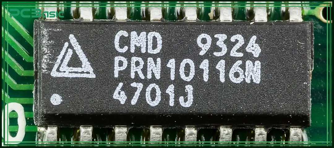
The Small Outline Integrated Circuit package (SOIC) is among the surface-mount integrated circuit SMD package types and has become widely used in modern electronics. It has a rectangular shape with pins or leads protruding from both sides.
SOIC offers several advantages over traditional packaging like dual-in-line packages (DIP). It is more compact in size, allowing for higher-density circuit boards. SOIC also facilitates better heat dissipation as it exposes the solder pads, increasing thermal performance.
SOIC has compact dimensions and at the same time, the distance between the pins is enough, being 1.27mm. This consistent standard pitch indicates that SOIC packages can be effectively assembled through the use of automated manufacturing techniques. Pins have a 'gullwing' profile to improve rigidity and support when the device is surface mounted on printed circuit boards.
Body widths of typical SOIC packages can vary between 3.9 mm for the smallest SOIC-4 package to 11.8 mm for larger SOIC packages with many pins. The overall length also differs based on the number of pins as well. All the packages in the SOIC family are physically different, but they all have the same pin spacing of 1.27 millimeters.
SOIC is currently one of the most widely used SMT packages because of the benefits it offers over older packages like the DIP. This is made possible because, while the correct pin pitch is definitive, the shape and size of the solder pads may be standardized, hence allowing the board to be assembled on production lines. This makes it possible to get circuits with higher integration densities in a single circuit board.

Time is money in your projects – and PCBasic gets it. PCBasic is a PCB assembly company that delivers fast, flawless results every time. Our comprehensive PCB assembly services include expert engineering support at every step, ensuring top quality in every board. As a leading PCB assembly manufacturer, we provide a one-stop solution that streamlines your supply chain. Partner with our advanced PCB prototype factory for quick turnarounds and superior results you can trust.
Taking a closer look at the key structural elements that define an SOIC package:
This robust but streamlined design makes SOICs amenable for high volume manufacturing while enabling miniaturization.
These are some of the key advantages that have made SOIC packages a standard choice:
● SOICs maximize component density on circuit boards with a miniature rectangular footprint.
● SOICs enable shorter trace lengths for improved electrical performance with less inductance and capacitance than older through-hole designs.
● The exposed thermal pad improves heat transfer from the die to the PCB, ensuring reliable operation even at higher power loads.
● As a JEDEC and EIAJ-standardized package, SOICs are fully compatible with automated pick-and-place and reflow soldering used in high-volume production.
● Mass manufacturing processes have reduced SOIC costs, and combined with their small size and high yields, they offer a cost-effective solution.
● The plastic-molded construction protects the die from damage and environmental factors like humidity better than exposed through-hole or LED chips.
Due to their versatility and widespread adoption of standards, SOIC packages are used in various applications across many industries.
These are some of the main applications.
SOIC is commonly found in smartphones, laptops, tablets and other consumer electronics. Its small size makes it well-suited for electronics that require component miniaturization. Microprocessors, memory chips, logic devices and more are often packaged in SOIC.
SOIC's reliability and resistance to vibration and thermal cycling make it popular for use in automotive applications like engine control units, infotainment systems, and advanced driver assistance components. Its wide operating temperature range accommodates the thermal demands of automotive applications.
The ability of SOIC to withstand harsh conditions also finds usage in industrial equipment such as factory automation devices, laser cutting machines, 3D printers, power tools and more. SOIC-packaged integrated circuits provide robust functionality in industrial environments.
Precision medical devices like imaging systems, patient monitoring equipment and surgical tools leverage the high reliability and manufacturability of SOIC. Its small size also allows for the miniaturization of medical technology.
SOIC is widely used in networking routers, switches, base stations and other equipment that form the backbone of wireless and wired communication systems due to its high-density performance in applications.
SOICs offer an ideal balance of size, performance, and cost for a diverse set of digital, analog, and mixed-signal applications.
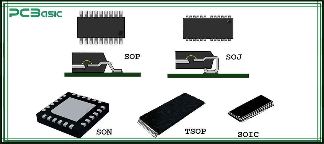
There are several variants of the basic SOIC package that exist with minor modifications suited to different needs. Here are some of them.
|
Variant |
Description |
|
SOIC Wide/Maxi |
Wider body for more pins or power ICs |
|
TOP |
Even smaller "thin-shrink" package |
|
SHOP |
A more compact "shrink" version of SOIC |
|
MSOP |
Extra-small "mini" package |
|
SOJ |
J-leaded gullwing pins for easier inspection |
|
FLSOIC |
Low-profile flat leads version |
|
ESOP |
Enhanced electrical performance |
|
LSOIC |
Lead-less version without connecting pins |
These variants improve on the baseline SOIC design for applications requiring enhanced density, electrical specs, or form factors. They maintain pin compatibility with the original SOIC footprint.

The SOIC package competes directly with and is an extension of several other integrated circuit packaging solutions.
Let's take a deeper look at how SOIC compares to some popular IC package types:
The TSSOP is considered a modification of the SOIC package type intended for higher-density applications. As the name suggests, it is less tall than other packages of standard small outline IC (SOIC) packages.
TSSOP bodies are up to 35% smaller with the same pin count. This allows more integrated circuits to be included in the same zone of the printed circuit board.
However, achieving tighter tolerances leads to increased manufacturing costs for TSSOPs. They also have a comparatively lower mechanical strength because package walls are thinner.
Any application that requires the smallest possible package at a reasonable cost prefers TSSOP to SOIC. These include cellular phones, tablets, and other portable and compact nature devices.
The Small Outline Package (SOP) shares the exact outline dimensions as SOIC but is specified with a broader body and larger pin/lead pitch spacing.
The expanded footprint accommodates fewer total pins, typically 8-20. This makes SOP well-suited for older linear and general-purpose analog ICs that don't require high densities.
Thermals are also better than SOIC due to lower component stacking and wider lead spacing, which allows more heat to dissipate.
Where thermal management or a small pin count are priorities, an SOP package can still be preferable over SOIC despite losing the density benefits. Joint replacements include voltage regulators.
However, prior to the emergence of surface mount technology, the Dual In-line Package (DIP) was the most widely used package using the through-hole mounting technique from the 1960s up to the early 1990s.
DIP IC was replaced by SOIC by removing pins that were inserted into holes in the board. This meant that more compact circuit layouts had a considerably lower profile.
Self-alignment and automated reflow were also implemented over manual through-hole soldering, which enhanced manufacturability.
Backward compatibility was the biggest problem for DIP's continuation. SOIC emerged as the dominant package because while it encouraged miniaturization, it did not hamper production's scalability.
Quad Flat Packages (QFP) offer even more terminal count than SOIC because they have leads on all four sides of the package.
This is considerably more than the maximum of about 50 pins for SOICs; QFP densities range from 100 to over 1,000 pins. This makes them good for complex microprocessors, FPGAs, and similar elements.
However, QFP manufacturing requires a more complex leadframe assembly and molding process than the designs of SOIC.
This is usually a common scenario, although it's not always the case; they are generally cheaper than the former. SOIC continues to be the preferred packaging solution when size, cost, and other factors are considered.
Since its introduction decades ago, the SOIC package has become a ubiquitous standard in billions of electronic products worldwide. Its compact dimensions, affordable manufacturing, and reliability advantages have made it ideal for cost-sensitive consumer, automotive, and industrial applications.
Several variants of SOIC sustain its relevance today across diverse technologies. Improvements in miniaturization by all package manufacturers will keep pushing the integration boundaries. However, the tried and tested SOIC form factor will likely remain popular in entry-level to mid-range electronics in the foreseeable future. With its near-perfect blend of size, performance, and economics, SOICs continue delivering practical solutions to integrating more circuits into progressively smaller spaces.

Assembly Enquiry
Instant Quote
Phone contact

+86-755-27218592
In addition, we've prepared a Help Center. We recommend checking it before reaching out, as your question and its answer may already be clearly explained there.
Wechat Support

In addition, we've prepared a Help Center. We recommend checking it before reaching out, as your question and its answer may already be clearly explained there.
WhatsApp Support

In addition, we've prepared a Help Center. We recommend checking it before reaching out, as your question and its answer may already be clearly explained there.