Global high-mix volume high-speed PCBA manufacturer
9:00 -18:00, Mon. - Fri. (GMT+8)
9:00 -12:00, Sat. (GMT+8)
(Except Chinese public holidays)
Global high-mix volume high-speed PCBA manufacturer
9:00 -18:00, Mon. - Fri. (GMT+8)
9:00 -12:00, Sat. (GMT+8)
(Except Chinese public holidays)
HomePage > Blog > Knowledge Base > PCB Lamination Process | A Comprehensive Guide
Today’s electronics have many parts in common and at the center is the PCB, from the simplest of cell phones to the most sophisticated medical devices. What’s worth mentioning is that particular factors like the PCB lamination process tend to more wide ranging scope of influence over the functionalities of a PCB today. Another important aspect that should be taken into account is that it creates both a structural and design solid fit, even within the most complex designs. Laminate PCBs would invariably collapse in hostile environments that require high performance due to poor lamination techniques.
Get familiarize with all that comes into play for the effective lamination of a PCB of your choice and its significance so that you don’t have to depend on the industry. These have a huge amount of applications based on the niche including but not limited to PCB fabrication, electrical engineering, and the most interesting working with electronic as a hobby.
This guide will help you understand how reliable and effective a PCB can actually be in real life.
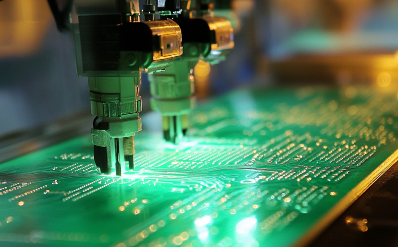
It's fascinating how that same computer would look totally different in a makeover, the lamination process works majorly by taking a resin, copper and many more and putting it through a PCB Lamination machine. This has a key role in the metallurgy multilayer of dense PCBs in the high speed case packed electronic devices. Whenever there is a lamination, the layers become one by adhering to each other, which in return enhances the board's reliability and efficiency.
For the implementation of multilayered PCBs, compact and multilayered designs are imperative working with multilayered PCBs. This is a feature regarding the lamination process in situations where it is necessary to stack a layer or a number of layers horizontally over a large area while meeting all the electrical or mechanical requirements.
The lamination of PCBs is also of cushioning effect and serves to fix the boards to one another and protects separation or bending during the application. It prevents the deformation of the board even under excessive thermal and mechanical stresses. Lamination reduces the risks of interlayer conductor tracing with a PCB which can lead to detrimental impacts on the electrical performance of PCBs problems by guaranteeing that electrically conductive portions of PCB layers are separated from one another which insulation altogether improves the performance of PCB. In addition, it gives mechanical strengthening, hard and durable properties of PCB.
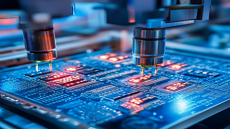
Multilayer PCB Lamination
This is a method that is required for complex designs whereby multiple layers of copper with substrate elements are bonded or laminated to form a single PCB laminate board. This process is important in the production of printed circuit boards required in high density circuit applications, such as those found in smart phones, aerospace electronics and medical devices.
This is further justified by the fact that the shrinking size of electronics components requires multilayer lamination since this increases the number of the circuits that can be contained in a limited area.
Sequential PCB Lamination
This category of these PCB laminate types generates a high density interconnect layout by sequentially nesting additional layer as per requirement to a standard layer count PCB. It consists of multiple lamination cycles in which an additional layer is added to the parent one.
This is most beneficial for PCB designs, which require multiple sophisticated functions but need to be small in size. In addition, because of features such as blind and buried vias, HDI PCBs usually use a sequential stacking method.
Teflon (PTFE) Microwave Lamination
Construction techniques also utilize Teflon laminated materials for microwave and telecommunication radar circuits requiring high dielectric absorption because of Teflon’s high thermal stability. In order to improve the quality and working performance of the final product, the lamination of Teflon requires a very controlled temperature and pressure environment.
Double-side laminated PCBs soldering opportunity
In lamination, copper foil is placed on both surfaces of the core creating a double sided PCB. Notably a PCB having copper traces on both sides. This type is suitable for simple electrical designs that do not have a lot of traces making it necessary to reduce layers and hence the cost of fabrication of PCBs.
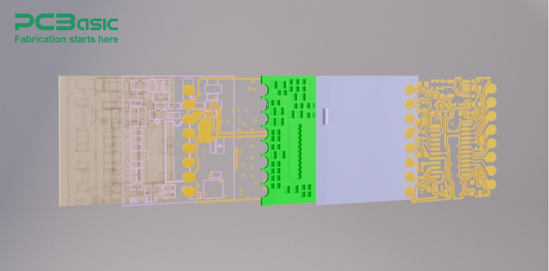
Preparation of PCB Layers
The first stage is to prepare such surfaces - copper and substrate - by cleaning and then depositing the desired layers. The interface layers are wiped clean so as to provide good bonding surfaces. If it sticks, the polymer layer will help during the lamination step and also relieves stresses in the finished part.
Making up of Parts
The next step is to arrange operationally ready copper and ready polymeric sheets in proper order. The bonding between the copper sheets is facilitated by pre-preg between the sheets. These pre-impregnated sheets should be correctly and evenly assembled so that the laminate PCB board meets the desired functions.
Vacuum Pressing
This guarantees that the mechanical and electrical characteristics of laminate board are in the best show state and it achieves effective distribution of stress in the PCB laminate and without voids in the assemblies.
Autoclave Lamination
When a working temperature is reached and appropriate pressure is applied, it results in the thermosetting resin curing, thereby solidifying the structure as well as laminating various layers together. The desired parameters for the process, including pre-preg temperature and pressure, are controlled to be at materially the same level.
Degassing
The last step is a procedure, which removes all other gases that may be remaining entrapped in the other layers. This step is critical to be performed as these en trapped gases may form ‘bubbles’ instead of laminate, which can rather defeat the purpose of the laminated PCB.
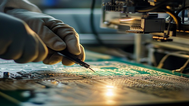
Temperature Control: The resin can be scorched at elevated temperature, and under-cured in certain areas when the temperature is too low. Consequently, the temperature of the copper clad laminate during PCB lamination must be controlled in accordance with the requirements in the specification.
Pressure Management: One of the properties of the PCB lamination process is the fact that there is a laminating sub-process of uniform pressure application which enables the laminated board being assembled to have vectored pressure in the assembly.
This process is called pressure control which is rather important. Failure of applying the required amount of pressure or applying an excess has negative effects on the board for example warpage or irregularity in the PCB laminate thickness.
Time Considerations: Each layer should dry together with the laminate, not after, within a certain amount of time; otherwise, too many bubbles will form, and the resulting product will not be of the highest quality.
This is because it requires a lot of heat and pressure which would be required for bonds to be formed but due to the limited time span did not happen resulting in poorly laminated multilayer structures.
Thermal Expansion During Lamination: Despite the wide variation in understanding the benefits of each panel, the thermal properties of bonded materials and bonded surfaces must be considered prior to making a decision. Neglecting this leads to damages associated with delamination and stress caused by the thermal shock, which generally reduces the durability of the laminate.
Material Compatibility
Selecting materials that have compatible mechanical and thermal characteristics is highly recommended. If such materials are not selected, problems such as delamination or thermal stresses are likely to occur which will in turn compromise the life span of the laminate PCB board.
Number of Lamination Cycles
For every given PCB design, the number of PCB lamination cycles will depend on the complexity of lamination cycles. The more the lamination cycles a PCB goes through the more cost and time are incurred but at the expense of higher performance. It is always a matter of performance versus cost.
Design Considerations
The design parameters, thickness of vias and their density, trace running density and the number of layers decides the requirement of layering. Eliminating such issues ensures that smooth PCBs are realized, thereby saving the company a great deal of money that is spent on repairs and replacements during PCB lamination.
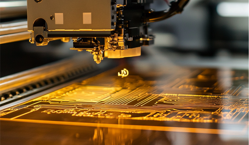
Sequential Lamination of HDI PCB-Focused Boards
The late stitching of circuits is very important in the logic board of the base and the receiver of the focal multiplexer HDI PCB. It enhances density and circuit interconnections and increases the relative number of cycles to the PCB lamination. This procedure is most suitable for targets such as mobile phones or medical smart devices.
Innovative Methods
The insertion of innovative features such as the use of halved fiber, laser, and digital production enhancing techniques greatly influences the production of PCB laminate. Such processes indeed provide time savings, increased degree of accuracy, and economic rationality, which are very critical in advancing contemporary technologies.
Scanning Acoustic Microscopy (SAM): SAM aids in identifying shortcomings, such as the separation of layers or voids in the internal planes of a material (which is the laminated part of the circuit board). It is an advanced non-destructive testing technique.
Interconnect Stress Testing (IST): The strength of the interconnections is ascertained under extreme temperatures and high mechanical loads using the Interconnect Stress Test. It is especially useful in locating the weak areas of voluminous multilayered PCBs with heavy heat applications.
Solder Float Testing: The float soldering test is used to remove the effect of lamination when soldering and reduces any possibility of the PCB lamination from pulling off or tending during the time of assembly.
Reflow Simulation Testing: This method simulates stresses that will be experienced in the actual copper clad laminate PCB soldering. With this step, even first time flooding of PCBs and laminates can be achieved thus widening the scope of reliability testing in practical situations.
Delaminating – This occurs when the air surrounds the composite irrecoverable layers, is laminated under high pressure, or if the adhesion is too weak. In turn, this may lead to internal electrical and mechanical weaknesses in the PCB.
CTE Mismatch – Due to Inherent thermal cycles, certain composite panels may heat or cool unevenly and thereby be under strain, leading to cracks. Such stress load may cause cracks or even delaminations, leading to the formation of displacement inside the laminate PCB board which results in diminished reliability of the component.
Misalignment – If the alignment of layers does not take place as per the requirements, then the circuits will take into reliance of redundancy and vice versa. When it comes to putting the sandwich together, minimizing the costs associated with the manufacturing process requires accurate aligning of every single element.
Design Guide for Sequential Lamination
There are good reasons as to why the HDI PCBs takes a long time in being finalized. There is a need in designing a more efficient layout that allows for via stacking and layers to be placed in order. At the same time the frame is preserved even though the sequential lamination allows for more complex designs to be made by PCB laminate manufacturers.
How to Improve HDI Reliability?
The HDI PCBs can be made more reliable if the PCB laminate suppliers are advised to use high quality PCB laminate materials, keep lamination parameters under control and evaluate HDI boards. Such strategies guarantee uniform resilience and quality.
The PCB lamination process is one of the most crucial electronic manufacturing process steps enabling high density design as well as highly reliable designs which are common in most digital devices. With this knowledge, you are more likely to make better designs and better equipment.
Increasing the complexity of the system does not necessarily increase its quality. This guide explains how to increase the performance of technology in compact modular plates. Related technologies include printed circuit boards and laminated HDI boards.
Hence, in figurative sense, I would say that performing, say, PCB trim and fill should be done with proper thinking, or if PCB lamination is done right, PCB design & creativity can reach new heights. But I'd rather highlight it from the other side. One need to understand that having this skill set constitutes a prerequisite to make highly practical laminate boards which are capable of surviving the hurricane of changes of the modern technologies.
Assembly Enquiry
Instant Quote
Phone contact

+86-755-27218592
In addition, we've prepared a Help Center. We recommend checking it before reaching out, as your question and its answer may already be clearly explained there.
Wechat Support

In addition, we've prepared a Help Center. We recommend checking it before reaching out, as your question and its answer may already be clearly explained there.
WhatsApp Support

In addition, we've prepared a Help Center. We recommend checking it before reaching out, as your question and its answer may already be clearly explained there.