Global high-mix volume high-speed PCBA manufacturer
9:00 -18:00, Mon. - Fri. (GMT+8)
9:00 -12:00, Sat. (GMT+8)
(Except Chinese public holidays)
Global high-mix volume high-speed PCBA manufacturer
9:00 -18:00, Mon. - Fri. (GMT+8)
9:00 -12:00, Sat. (GMT+8)
(Except Chinese public holidays)
HomePage > Blog > Knowledge Base > HASL vs. ENIG: How to Select the Right PCB Surface Finish
Modern electronic devices have received a facelift since printing circuit boards were invented. Printed circuit boards have improved electronic devices' performance, reduced sizes, and enhanced product durability. These qualities have been enhanced through more advanced surface finishes. Many surface finish methods exist, but the most common ones are Hot Air Solder Leveling (HASL) and Electroless Nickel Immersion Gold (ENIG). All these surface finish methods are essential, and one can only choose based on a specific area of use. This article introduces you to both HASL and ENIG methods of surface finish in detail and enables you to choose the one suitable for your product.
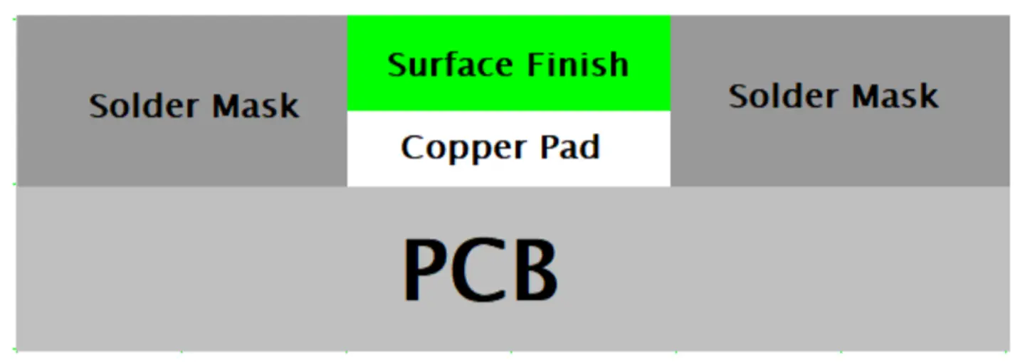
HASL stands for Hot Air Solder Leveling. It is the oldest and most commonly used PCB surface treatment and finish method. This method involves coating the PCB's copper tracks with molten solder. The molten solder comprises 37% Lead and 63% Tin, added to the soldering material.

Figure 1: Structure of the PCBs Showing HASL Surface Finish
To better understand HASL, let us go through the step-by-step processes involved.

Figure 2: Step-by-step HASL Process
· Pre-cleaning and treatment: The first step involves cleaning the PCB to remove dirt, debris, and oxidized copper layers.
· Flux coating: Flux material is applied to the PCB before the soldering process starts. Its function is to prevent oxidation and improve solder adherence during the soldering process.
· Preheating: The PCB is preheated at an average temperature of 150oC to ensure thermal stability, eliminate thermal shocks, and prevent the oxidation process. This process prepares the PCB for the molten solder immersion step.
· Solder Bath Immersion: The PCB is then submerged in a solder bath heated to about 265oC. This process ensures that all the exposed copper areas are coated.
· Hot Air Levelling: After immersion, the PCB is removed from the bath and passed through hot air knives. The process removes excess solder and achieves a uniformly distributed flat coat.
· PCB Cooling: The board is given a few minutes to cool. The cooling process allows the uniformly distributed solder to solidify.
· Post-Cleaning and Inspection: At this level, all the remaining debris is removed from the surface of the PCB. The board is also subjected to an inspection process to ensure that the expected result is achieved.
Two types of HASL PCB surface treatments exist: Lead-based and Lead-free HASL.
· Lead-Based HASL: This process uses a tin-based alloy, where tin, at 63%, is mixed with lead, at 37%. RoHS limits this process due to its environmental unfriendliness.
· Lead-free HASL: This process uses lead-free solder bath alloys. Instead of lead, copper strengthens the tin. The RoHS most preferred this method.
Below are the advantages of using HASL in the PCB surface treatment:
· Cost-effectiveness: HASL is one of the most economical and affordable PCB treatment methods.
· Durability: With HASL and proper storage, the product is guaranteed a longer shelf life than other methods.
· Solderability: HASL offers good solderability, ensuring a strong bond after completing the PCB soldering process.
· Visual inspection: With HASL, the user can visually inspect the end product and identify any flows that occurred during the process.
After using the HASL method of surface finish, expect the following disadvantages to occur:
· Flatness defects: Achieving the perfect flatness during hot air leveling is almost impossible, which might pose a challenge to components with small pitches, such as the BGAs.
· RoHS environmental concerns: Lead-based alloys HASL are an ecological and health hazard, making the process uncompliant with the RoHS standards.
· Thickness variation: HASL can have PCBs with variations in thickness, which can introduce issues in end products.
· Not preferred for more advanced PCBs: Some PCBs, such as high-speed and high-frequency circuits, require highly accurate finishing, which HASL cannot deliver. Instead of HASL, ENIG is preferred.
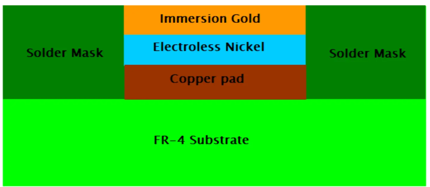
ENIG, the Electroless Nickel Immersion Gold, is now the most widely used PCB surface treatment method. It consists of two layers that achieve a flat and solderable platform. The process is possible by forming a 0.05 to 0.2mils flat layer of Nickel deposits to cover the copper tracks and pads. Then, the final layer of gold, ranging from 0.05 to 0.15 mils, is created to cover the nickel layer.
For optimal performance, the manufacturer must attain the required thickness of the ENIG layer. A nickel layer of standard thickness protects the gold layer from diffusing into the copper traces and pads. The gold layer offers a surface for proper solderability. Manufacturers opt for an ENIG surface finish when producing highly reliable products; performance is given great attention. This includes areas such as the medical, defense, and aerospace industries.

Figure 3: PCB with an ENIG Surface Finish
ENIG is made possible through the following step-by-step process:

Figure 4: Step-by-step Processes in ENIG
· Pre-cleaning: The PCB is passed through a thorough pre-cleaning process to remove debris, dirt, and other contaminants that might be present on its surface.
· Etching: The PCB undergoes an etching process to remove any excess copper on the surface. The process involves a unique acid solution that dissolves copper while maintaining the rest of the circuitry.
· Electroless Nickel Plating: The board is dipped in an electroless nickel-soluble bath to deposit a skinny layer of nickel on the surface of the copper tracks and pads. This layer protects the gold layer from diffusing into the copper pads and tracks.
· First Rinsing: The PCB undergoes rinsing, which is necessary for removing the extensively deposited nickel solution on its surface.
· Immersion Gold Deposition: The PCB is dipped into a gold solution bath. This gold solution reacts with the previously formed nickel layer, thus depositing a skinny gold layer on the surface. The formed gold layer is intended to improve solderability.
· Final Rinsing: A final rinsing removes excessive gold solution on the PCB surface.
· Post-cleaning, Drying, and Inspection: The PCB undergoes vigorous post-cleaning and drying. It is then inspected to ensure no defects are incurred during manufacturing.
· Surface flatness: A flat surface is easy to achieve, making it suitable for BGAs and SMT components.
· Durability: ENIG is highly durable because nickel is robust, making the product highly wear-resistant.
· Corrosion resistance: Gold has a corrosion-resistant ability, protecting corrosion-prone nickel.
· Trace texture: ENIG gives fine traces, which is highly preferred in manufacturing high-density interconnect PCBs.
· Environmental compliance: The process is approved by the RoHS standards due to its nature of environmental protection. ENIG does not use lead materials.
· Shelf life: ENIG has an oxidation protection feature, thus giving PCBs a longer shelf life.
· Cost: As compared to HASL, ENIG is more expensive.
· Process complexity: ENIG is a more complex process. It requires special attention and equipment to achieve.
· Defects: ENIG is attacked by the black pad defect, which occurs when nickel plating creates failures in solder joints.
Thickness limitations: The plated gold is always skinny, which might not be advised for some application areas.
|
FEATURE |
HASL |
ENIG |
|
Cost |
Low |
High |
|
Corrosion resistant |
Moderate |
Highly resistant |
|
Surface finish |
Uneven surface |
Very flat Surface |
|
Thermal resistant |
Moderate |
Very high |
|
Environmental protection |
Moderate to high, depending on the choice between the two types of HASL |
High environmental friendly |
|
Area of Application |
Industrial, Consumer electronics. |
Aerospace, HDI PCBs, and Automotive. |
Selecting the correct surface finish during PCB manufacturing can be challenging. Manufacturers consider various factors to achieve this and below are some of the factors to consider in the process.
· Application area: ENIG is considered for projects that require a high level of reliability and high-density PCBs. If your product has fewer design requirements and should be cost-effective, settle for HASL.
· Budget constraint: This question is very crucial before you choose between ENIG and HASL. Low-budget products cannot settle for ENIG, where HASL can provide the best output at a cheaper price.
· RoHS Standards Consideration: ENIG or lead-free HASL are considered where environmentally friendly products are required. The processes adhere to the RoHS standards.
· The assembly needs: Fine pitch and small components will make you opt for an ENIG surface finish due to its surface flatness.
HASL vs. ENIG both come with several benefits and limitations. This makes a manufacturer make an informed choice on which surface finish method to use. HASL brings cost-effectiveness and frequently available solutions, which makes it an option in simple PCB designs. ENIG brings in the best flatness, reliability, and high aesthetic features that are much preferred in high-performance and advanced PCBs. To make the best choice between the two, you must understand your project requirements so that your choice of surface finish can be the best choice for meeting your end product goal.

Assembly Enquiry
Instant Quote
Phone contact

+86-755-27218592
In addition, we've prepared a Help Center. We recommend checking it before reaching out, as your question and its answer may already be clearly explained there.
Wechat Support

In addition, we've prepared a Help Center. We recommend checking it before reaching out, as your question and its answer may already be clearly explained there.
WhatsApp Support

In addition, we've prepared a Help Center. We recommend checking it before reaching out, as your question and its answer may already be clearly explained there.