
Global high-mix volume high-speed PCBA manufacturer
9:00 -18:00, Mon. - Fri. (GMT+8)
9:00 -12:00, Sat. (GMT+8)
(Except Chinese public holidays)





HomePage > Blog > Knowledge Base > Machine Vision Camera PCB Assembly: How the Boards Are Built and Tested
1. Inside a Machine Vision Camera PCBA
2. What Makes Machine Vision Camera PCB Assembly Challenging
3. The Machine Vision Camera PCB Assembly Process
4. Testing and Verifying the Assembled Board
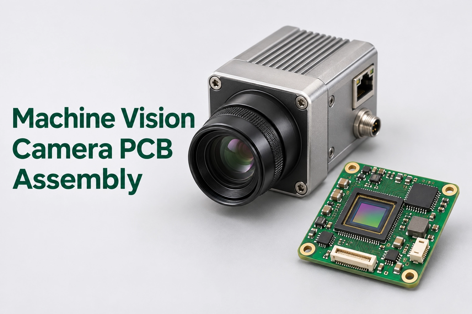
At the core of every industrial camera is its electronic board assembly. While lens optics and vision software receive much of the public focus, hardware stability directly governs image quality, data throughput, and field lifespan. For hardware engineers and procurement specialists, understanding how a machine vision camera PCB assembly is built, protected, and verified ensures smooth vendor collaboration and repeatable manufacturing quality.
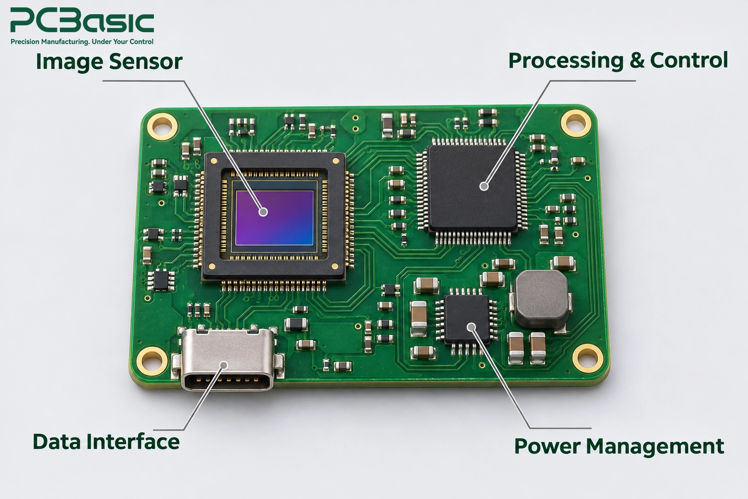
An industrial machine vision camera PCBA hosts the critical components required to capture light, process image data, and transmit digital signals to a host system. Depending on the camera's resolution, target frame rate, form factor, and budget, the circuit architecture can range from a single rigid board to a compact multi-board assembly.
A standard industrial camera architecture generally divides functional responsibilities across four primary subsystems:
• Image Sensor Subsystem: Contains the CMOS or CCD image sensor and its immediate support circuitry. The primary layout objective here is minimizing local noise and trace cross-talk, as electrical interference near analog front-end signals directly degrades image clarity.
• Processing & Control Unit: Responsible for processing raw pixel streams, applying Bayer demosaicing (where applicable), and managing camera firmware. High-performance designs may integrate an FPGA, SoC, or dedicated DSP, whereas simpler entry-level cameras utilize streamlined microcontrollers or fixed-function image signal processors (ISPs).
• Power Management Subsystem: Converts and filters incoming power into clean, low-ripple rails. Stable power distribution helps minimize power-related noise and maintain stable operation in temperature-sensitive areas.
• High-Speed Interface Layer: Converts internal pixel streams for external interface standards such as GigE Vision, USB3 Vision, Camera Link, or CoaXPress. Differential routing and impedance matching are structured specifically to support the cable length and streaming data rates specified for the camera design.
Building a machine vision camera PCB requires addressing specific assembly risks that differ from general-purpose consumer electronics. Manufacturing lines must actively mitigate contamination, thermal stress, and mechanical alignment risks based on the specific engineering drawings of the product.
Particulate contamination on an image sensor PCB poses a major yield risk when dust, lint, or airborne flux residue settles directly onto the optical cover glass, image sensor window, or internal optical path. Contaminants located in this optical path shadow the pixel array, potentially causing visible dark spots or shadows in captured images. Assembly procedures must prioritize component manufacturer-approved protective tape or caps, clean environments, and appropriate handling protocols during placement and inspection, noting that certain sensor guidelines restrict the use of protective films directly on active glass surfaces.
High-speed processing chips and image sensors generate localized heat during continuous operation. Heat must be systematically conducted away using thermal vias, ground planes, or thermal interface materials (TIMs) to keep component junction temperatures within rating. Additionally, hardware designers and assemblers must evaluate coefficient of thermal expansion (CTE) differences between ceramic sensor bodies, BGA packages, and FR4 substrate materials. Managing the resulting thermal-mechanical stresses reduces long-term thermal-mechanical fatigue on solder joints.

As pixel clocks and multi-gigabit serialization rates increase, maintaining trace geometry, continuous reference planes, and controlled impedance becomes critical across the camera PCB. Discontinuities can lead to packet drops, reduced transmission distance, or electromagnetic compatibility (EMC) test failures.
It is important to distinguish SMT placement precision from final optical alignment:
• SMT Component Placement: Ensures that the image sensor package and passive components sit squarely on their pads according to approved assembly drawings, component specifications, and applicable acceptance criteria before reflow.
• Optical Alignment: Focuses on the precise positioning of the sensor's active pixel area relative to the lens mount axis and flange focal distance. Depending on optical sensitivity, alignment may rely on mechanical pin registration or active optical alignment during final assembly according to design drawings.
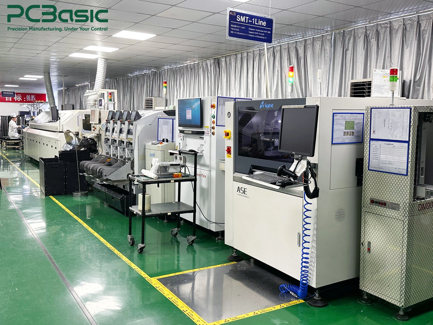
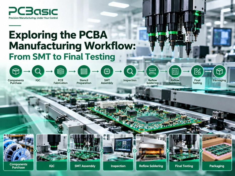
A reliable industrial camera PCB assembly requires thorough front-end documentation checks, controlled SMT processing, and continuous inspection. Electronics manufacturing service (EMS) partners structure assembly around clear customer specifications, bill of materials (BOM) validation, and full batch traceability.
Before production begins, engineers review Gerber layers, BOM files, and component data sheets. Moisture-sensitive devices (MSDs) and sensitive optical sensors undergo baking cycles when required by their moisture sensitivity level (MSL), storage history, and manufacturer specifications, while board stackups and mechanical drawings are cross-checked for fabrication readiness.
Solder paste is applied using precise laser-cut stencils or piezoelectric jet printing, chosen based on component pitch and prototype volume. Selective nano-coated stencils help maintain uniform paste release across fine-pitch pads, reducing the risk of solder bridging or insufficient volume under tight-pitch ICs.
High-speed pick-and-place equipment uses vision alignment systems to verify component orientation and package geometry prior to board placement. Special nozzles and controlled placement force prevent mechanical stress on delicate packages and sensor windows.
Boards pass through multi-zone convection reflow ovens configured with custom thermal profiles matched to the thermal mass of the assembly, solder paste requirements, and component temperature limits. Where specified for oxidation-sensitive components or dense packages, reflow can be conducted in a nitrogen (N₂) environment to promote wetting and potentially reduce void formation. Partnering with experienced providers like PCBasic ensures that these processes are backed by rigorous incoming material verification, controlled SMT lines, structured inspection protocols, and full batch traceability from prototype to production.

Post-reflow cleaning depends strictly on component compatibility. While standard boards may undergo automated washing to remove flux residue, assemblies featuring open optical paths, sensitive MEMS, or non-washable sensors require manufacturer-approved selective cleaning methods or exclusion from washing to safeguard sensitive components and optical surfaces.
Validating a machine vision camera PCBA requires combining conventional electronic hardware inspection with dedicated functional checks.
|
Testing Stage |
Inspection Method |
Key Target / Defect Screened |
|
Visual & Joint Inspection |
Automated Optical Inspection (AOI) |
Skewed components, missing parts, solder bridging, tombstoning |
|
Hidden Joint Inspection |
Automated X-Ray Inspection (AXI) |
BGA solder voiding, hidden pad bridging, barrel fill |
|
Electrical Continuity |
In-Circuit Test (ICT) / Flying Probe |
Open circuits, net shorts across programmed netlists |
|
Power & Interface Validation |
Functional Test Rig |
Voltage rail stability, boot sequence, host communication |
|
Image & Trigger Verification |
Controlled-Lighting / Test Target Setup |
Pixel anomalies, trigger timing response, frame rate stability |
AOI and AXI respectively inspect visible surface features and hidden solder joints beneath array packages after reflow, checking for component placement accuracy and solder voiding percentages.

In-circuit testing (ICT) or flying probe testing verifies net continuity, resistance, and capacitance according to the programmed test coverage, checking for short circuits between power and ground networks before applying operational voltages.
Once preliminary electrical checks pass, the machine vision camera module undergoes initial power-up verification to check voltage regulators for stable output and low ripple, and to verify proper host communication over GigE, USB3, or alternative interfaces.
Final operational acceptance testing evaluates image output under defined project conditions:
• Image Capture: Acquires images under specified illumination, exposure times, and host setups to evaluate baseline image output, pixel performance, and uniformity.
• Trigger Response: Where supported by camera design, hardware trigger inputs are pulsed to verify external trigger synchronization and timing latency.
• Continuous Transmission: Streams image data at designated resolutions, frame rates, and cable lengths over a specified test duration to verify stable transmission within allowable packet loss limits.
Manufacturing a reliable machine vision camera PCB assembly requires careful attention at every stage of production—from initial Gerber and BOM reviews to precise SMT placement, controlled reflow, and comprehensive functional verification. Addressing particulate control, signal integrity, and thermal demands early in the manufacturing cycle helps minimize production risks and supports manufacturing consistency.
When preparing your camera design for production, partnering with an experienced manufacturing provider streamlines the transition from prototype to volume assembly.
To request a manufacturing review or preliminary quote for your vision project, contact PCBasic with your project documentation—including Gerber files, BOM, assembly drawings, component handling guidelines, and target testing criteria.
Q1: What steps protect image sensor cover glass from contamination during assembly?
Protection strategies include using component manufacturer-approved protective tape or caps over the optical window during initial SMT processing, assembling in controlled clean environments, and carrying out manual optical inspections before final optics mounting.
Q2: When is nitrogen reflow recommended for camera board assembly?
Nitrogen (N₂) reflow may be specified following process evaluation for assemblies featuring dense BGA packages, fine-pitch ICs, or complex multi-layer designs where reducing solder oxidation, improving wetting, and potentially minimizing void formation under ground pads are priority requirements.
Q3: What documentation should procurement teams provide for PCBA quoting?
Procurement teams should provide standard Gerber files (or ODB++), a detailed BOM with manufacturer part numbers, assembly drawings, specific SMT placement tolerances, sensor handling instructions, and functional test specifications outlining voltage limits, interface protocols, and pass/fail criteria.

Assembly Enquiry
Instant Quote

Phone contact

+86-755-27218592
In addition, we've prepared a Help Center. We recommend checking it before reaching out, as your question and its answer may already be clearly explained there.
Wechat Support

In addition, we've prepared a Help Center. We recommend checking it before reaching out, as your question and its answer may already be clearly explained there.
WhatsApp Support

In addition, we've prepared a Help Center. We recommend checking it before reaching out, as your question and its answer may already be clearly explained there.
