Global high-mix volume high-speed PCBA manufacturer
9:00 -18:00, Mon. - Fri. (GMT+8)
9:00 -12:00, Sat. (GMT+8)
(Except Chinese public holidays)
Global high-mix volume high-speed PCBA manufacturer
9:00 -18:00, Mon. - Fri. (GMT+8)
9:00 -12:00, Sat. (GMT+8)
(Except Chinese public holidays)
HomePage > Blog > Knowledge Base > IoT PCB Assembly: Driving the Future of Connected Devices
The Internet of Things (IoT) is shaping the future of industries by connecting devices and enabling smarter solutions. At the core of every IoT device lies the PCB assembly, which ensures that electrical components are properly connected, and signals flow seamlessly. In this article, we will explore the importance of IoT PCB assembly, the challenges involved, and the role of IoT PCB manufacturers and suppliers in delivering high-quality assemblies for IoT applications, including medical IoT PCB assemblies.
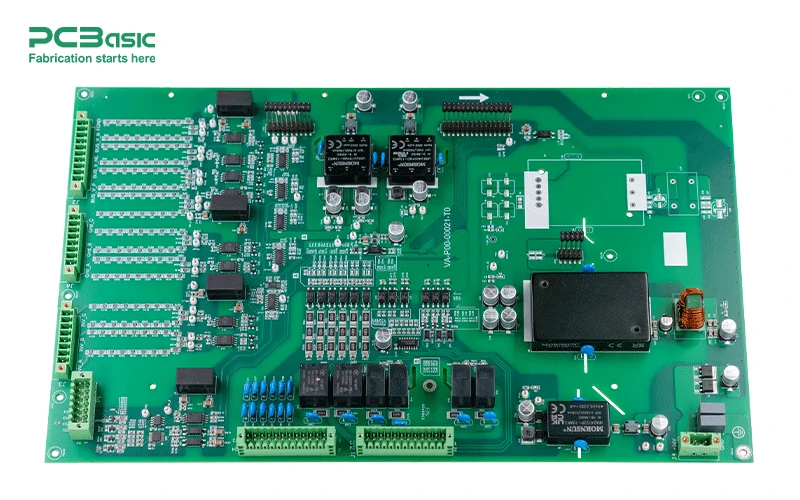
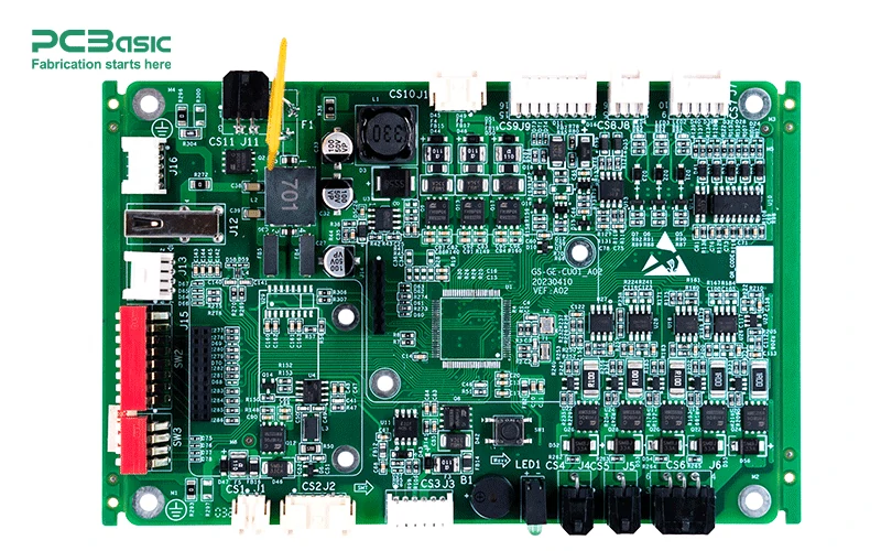
IoT PCB assembly refers to the process of assembling the components (such as resistors, capacitors, microchips, and sensors) onto a PCB to create a fully functional IoT device. This process involves several stages, including component placement, soldering, and testing, ensuring that the IoT device works reliably and efficiently.
The assembly process for IoT PCBs needs to be precise, as these devices are often used in critical applications where performance and reliability are crucial.

Connectivity: IoT devices rely on various forms of wireless communication such as Wi-Fi, Bluetooth, and Zigbee. The PCB assembly needs to ensure these components are perfectly integrated and can function as intended.
Power Efficiency: Many IoT devices, especially those in remote locations or battery-powered, need to minimize energy consumption. A properly assembled PCB with energy-efficient components ensures that these devices last longer without frequent recharging or battery replacement.
Compact Design: IoT devices are often small and need to be lightweight while containing complex systems. IoT PCB assembly must take this into account, optimizing space on the PCB to allow for advanced, compact designs.
The process of assembling IoT PCBs comes with its own set of challenges:
Miniaturization: As IoT devices become smaller, the components used on the IoT PCB need to be smaller as well. This increases the complexity of the assembly process, as the precision of component placement becomes even more critical.
Component Density: IoT devices often require a high component density on the PCB to incorporate sensors, communication modules, and power management components. This makes PCB assembly a delicate process that requires advanced techniques.
Reliability: IoT devices are often deployed in harsh environments where they need to function reliably over long periods. A high-quality IoT PCB assembly is essential to ensure that the device can withstand temperature variations, humidity, and other environmental factors.
Signal Integrity: IoT devices often require high-speed data transmission. Ensuring signal integrity on the assembled PCB is essential to avoid signal loss or interference, especially in wireless communication applications.
IoT PCB manufacturers and suppliers play a vital role in ensuring the successful assembly of IoT PCBs. Here's how they contribute to the process:
Component Sourcing: Reliable suppliers provide high-quality components that meet the specific requirements of IoT devices, such as low-power components for energy efficiency and robust components for durability.
Advanced Assembly Techniques: IoT PCB assembly requires precision. Manufacturers use pick-and-place machines for accurate component placement, reflow soldering for secure connections, and wave soldering for through-hole components.
Testing and Quality Assurance: IoT PCB manufacturers conduct a series of tests to ensure that the assembled PCB works correctly. Common tests include electrical continuity checks, functional testing, and thermal cycling tests to ensure the PCB performs under different conditions.
Packaging and Shipping: Once assembled and tested, IoT PCBs are carefully packaged to prevent damage during transit. For high-value or sensitive IoT products, manufacturers often use anti-static packaging and moisture protection.

Medical IoT PCBs require specialized assembly processes due to the critical nature of medical devices. Whether it’s for wearable health monitors, remote patient monitoring systems, or diagnostic equipment, these devices must meet the highest standards for quality and safety.
Key considerations for medical IoT PCB assembly include:
Compliance: Medical IoT devices must meet strict regulations and standards such as FDA requirements, ISO certifications, and CE marks. Manufacturers must ensure that the assembled IoT PCB is fully compliant with these standards.
Reliability: In healthcare applications, reliability is paramount. The assembly process must ensure that components are securely placed and that there are no soldering defects that could impact the device's performance.
Sterilization: Some medical IoT PCBs need to be sterilized before they can be used in medical environments. The assembly process may involve using specialized materials or techniques that can withstand sterilization procedures.
China has become a major hub for IoT PCB assembly due to its advanced manufacturing capabilities, cost-effectiveness, and high-quality standards. Many IoT PCB manufacturers in China are known for their expertise in automated assembly, ensuring that the IoT PCBs are assembled accurately and efficiently.
By choosing a trusted China IoT PCB supplier, companies can reduce production costs, access cutting-edge technology, and benefit from fast turnaround times. China-based suppliers are capable of handling high-volume orders while maintaining quality control and adhering to international standards.

IoT PCB assemblies come in various forms depending on the complexity and application of the device. The most common types include:
Single-Sided PCB Assembly: Typically used for simpler IoT devices, these are cost-effective and easy to assemble but have limited space for components.
Double-Sided PCB Assembly: Ideal for IoT devices with higher component density, double-sided PCBs allow for more components to be placed on both sides of the board.
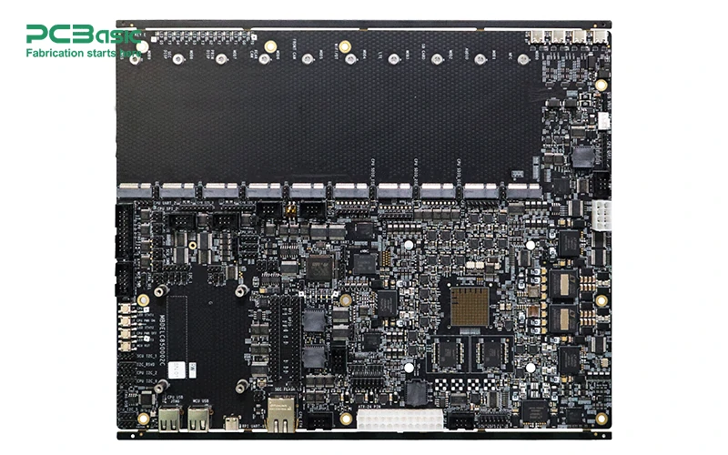
Multilayer PCB Assembly: Used in more complex IoT devices where higher component density and signal integrity are required. Multilayer IoT PCB assemblies are common in advanced medical devices, wearables, and industrial IoT systems.
Flexible PCB Assembly: Used in wearable IoT devices, these assemblies offer flexibility, enabling the PCB to bend or fold without damaging the circuitry.
Rigid-Flex PCB Assembly: Combining the benefits of both rigid and flexible PCBs, these are used in IoT devices that require both a compact, flexible design and robust mechanical strength.
The assembly of IoT PCBs is a critical step in the development of reliable and high-performance IoT devices. From sourcing components to assembly and testing, IoT PCB manufacturers and suppliers play an essential role in bringing innovative IoT solutions to life. Whether it's for consumer electronics, medical IoT applications, or industrial systems, the IoT PCB assembly process ensures that these devices work reliably and efficiently in the real world. Partnering with experienced IoT PCB manufacturers—especially those in China IoT PCB assembly—can provide the expertise and scalability needed to stay ahead in the rapidly growing IoT market.

Assembly Enquiry
Instant Quote
Phone contact

+86-755-27218592
In addition, we've prepared a Help Center. We recommend checking it before reaching out, as your question and its answer may already be clearly explained there.
Wechat Support

In addition, we've prepared a Help Center. We recommend checking it before reaching out, as your question and its answer may already be clearly explained there.
WhatsApp Support

In addition, we've prepared a Help Center. We recommend checking it before reaching out, as your question and its answer may already be clearly explained there.