Global high-mix volume high-speed PCBA manufacturer
9:00 -18:00, Mon. - Fri. (GMT+8)
9:00 -12:00, Sat. (GMT+8)
(Except Chinese public holidays)
Global high-mix volume high-speed PCBA manufacturer
9:00 -18:00, Mon. - Fri. (GMT+8)
9:00 -12:00, Sat. (GMT+8)
(Except Chinese public holidays)
HomePage > Blog > Knowledge Base > PCB vs PCBA: What's the Difference - PCBasic
A PCB (Printed Circuit Board) is a
bare board without components installed, mainly used to provide mechanical support
for electronic components and electrical connection pathways. PCBA (Printed
Circuit Board Assembly), on the other hand, is a finished circuit board that
completes component mounting and soldering onto the PCB, and it has complete
circuit functions. This essential difference is the core process of modern
electronic manufacturing and directly affects design choices and the
performance of the final product.
As electronic devices rapidly
develop towards high integration and miniaturization, a deep understanding of
the roles of PCBs and PCBA has become increasingly important. This article
explores the core concepts of printed circuit boards (PCBs) and printed circuit
board assembly (PCBA), providing an overview of their structures, manufacturing
processes, and main differences. By clearly understanding these elements,
professionals can make wiser decisions throughout the product development life
cycle and optimize performance and efficiency.
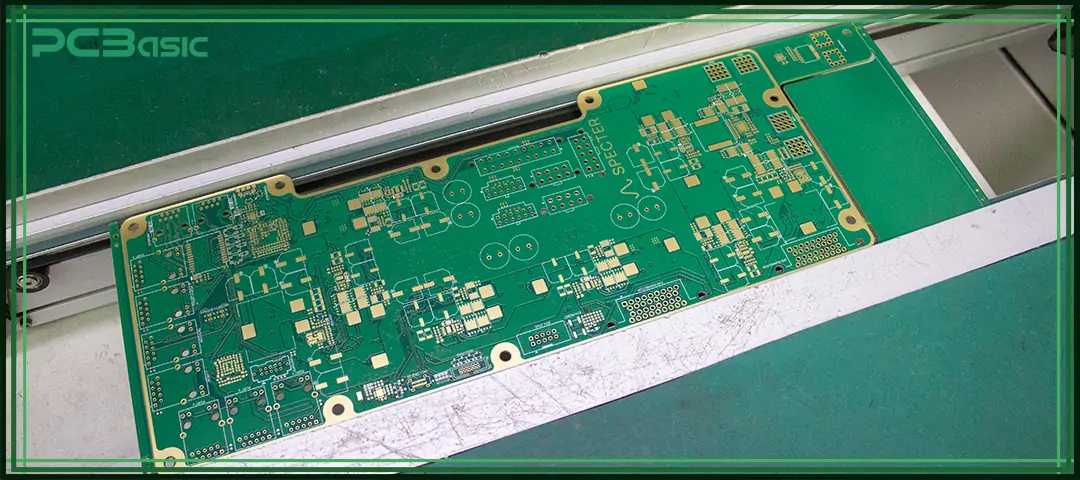
Printed Circuit Boards (PCBs) are slender panels crafted from insulating materials like fiberglass or epoxy resin. Their surfaces feature conductive traces, predominantly copper, which act as vital electrical conduits linking electronic elements such as resistors, capacitors, and integrated circuits.
A PCB's core role is to offer a firm, structured base for affixing and connecting these circuit components, allowing them to execute specific functions in an electronic device collaboratively.
PCBs streamline wiring complexities and bolster electronic device reliability. Leveraging PCBs, designers can fashion sleek, high-performance circuits that resist errors and simplify diagnostics.
Furthermore, PCBs deliver essential mechanical support, keeping components in place and precisely aligned. This stability is pivotal, especially in environments with significant vibrations or when devices endure physical duress.
PCB performance pivots on multiple determinants. The insulating material's thickness and variety, the breadth and gap between traces, and solder joint quality stand out as prime influencers. These elements shape the board's electrical traits, from resistance and capacitance to inductance, which, in turn, steer the device's overarching efficiency.
Hence, it's paramount to weigh these factors during the design and fabrication stages meticulously. This scrutiny ensures the PCB and its affiliated device function at their zenith potential.
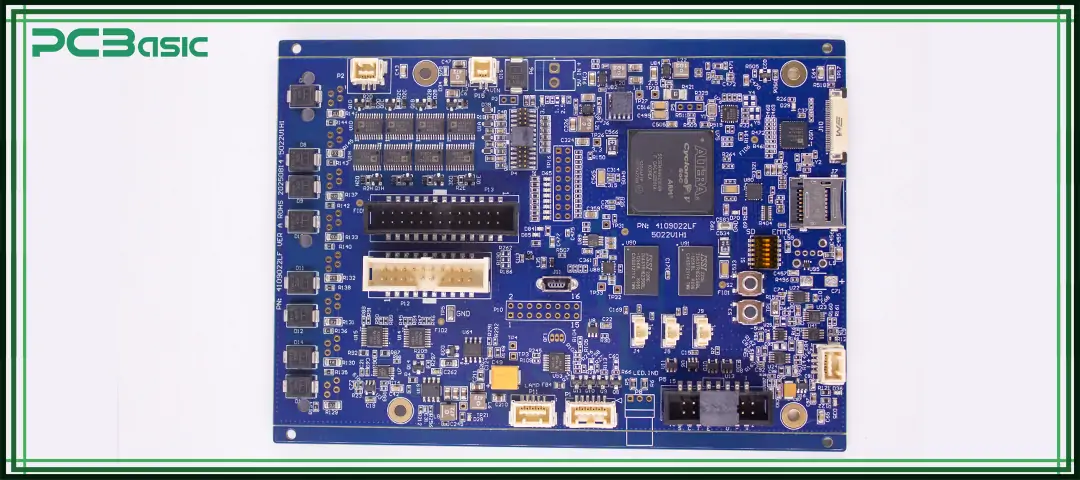
At its core, a Printed Circuit Board Assembly (PCBA) is more than just a simple PCB; it's an electronic component meticulously mounted and soldered, giving birth to a fully functional circuit.
Understanding the essence of PCBA takes us on a journey through the process termed "PCB assembly." This process, undeniably vital, serves as the cornerstone in the realm of electronic device production.
So, what's the raison d'être of a PCBA? In layman's terms, it offers a unified platform, a symphony stage where electronic components collaborate seamlessly. This unity ensures that the overarching device delivers on its promises, executing its tasks flawlessly.
So, a PCBA directs signals amongst components, all orchestrated by the device's schematic blueprint. Additionally, it is responsible for offering ground planes, voltage planes, and the intricate balance of impedance control, all pivotal for unwavering electrical performance.
However, the performance of a PCBA doesn't solely hinge on its design. Several external influencers come into play:
• The caliber of the components used
• The precision of the assembly process
• The integrity of those delicate solder joints
We just touched on how they're related not too long ago, but did you ever stop to ponder what sets them apart?
Now that I mention it, what differentiates a PCB from a PCBA? Let's look into their definitions, costs, and how they're made to understand this better.
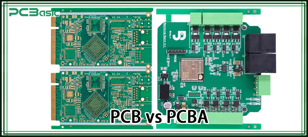
PCB: Refers to a Printed Circuit Board, which essentially provides the foundational structure with conductive traces on a non-conductive substrate.
PCBA: Stands for Printed Circuit Board Assembly. It's the advanced stage where the PCB has all the electronic components mounted and soldered onto it, making it a functional circuit.
PCB: Involves designing the board layout, etching conductive pathways, and drilling holes for potential component insertion.
PCBA: Takes a PCB to the next level by adding components like resistors, capacitors, and ICs. This involves processes like stencil printing, component placement, and reflow soldering.
PCB: Generally less expensive since it's just the board without any components.
PCBA: It tends to be more costly as it incorporates the cost of individual components and additional assembly processes.
Summary Table:
|
Aspect |
PCB |
PCBA |
|
Definition |
Board with conductive traces |
PCB with components attached |
|
Manufacturing |
Design, etching, drilling |
Stencil printing, placement, reflow soldering (SMT) |
|
Cost |
Less expensive (board only) |
More costly (board components plus assembly fee) |
|
Assembly Techniques |
Components are not mounted |
Can involve through-hole soldering, SMT, and BGA assembly |
When categorizing PCBs, there are a few things to consider. First off, we look at the assembly technique. Then, there's the complexity of the circuit to think about. And, of course, we can't forget the intended application.
So, diving right in, we've got three main types of PCBs.
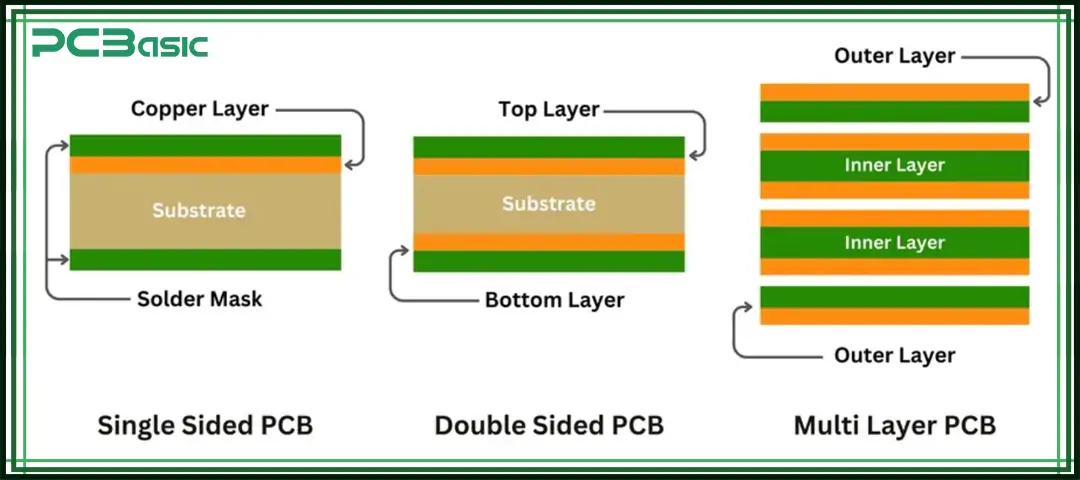
With just one insulating layer, these PCBs showcase conductive traces on a single side. Components? They snuggle right on the trace side, linking up either through the age-old through-hole (or, as some call it, thru-hole) soldering or the sleeker surface-mount technique.
If you're eyeing cost-effective options ideal for uncomplicated, low-density circuits or straightforward control setups, these are your go-to.
As the name suggests, they flaunt conductive traces on both faces of the insulator, paving the way for denser and more intricate circuit configurations. You can place components on either face, connecting them via the shiny plated-through holes (PTHs) or vias.
Now, if you're delving into realms like car tech, industrial controls, or comms gadgets, these PCBs are the ticket.
Remember, their versatility comes with a slightly heftier price tag, courtesy of the added steps to craft those PTHs and vias.
Envision numerous layers of insulators and conductive traces, all sandwiched together in a harmonious blend. They communicate between layers using PTHs or the more elusive blind and buried vias.
Ranging from a modest four layers to a staggering 30 (or even more!), these PCBs cater to the crème de la crème of electronics. Think high-octane computers, state-of-the-art smartphones, or cutting-edge medical tools.
They might be pricier and take longer to produce, but they're unbeatable when you need top-tier performance and have spatial challenges.
In electronics, every PCB type has its shining moment. Your choice hinges on several facets: circuit complexity, space inside the gadget, performance, and budget.
But with a solid grasp of these PCB types, making that perfect choice becomes a breeze for designers and engineers.
A PCB board is more than just a base for attaching electronic components. It's a meticulously designed platform that consists of multiple layers and elements, ensuring seamless functionality. Here are the foundational components of a bare PCB:
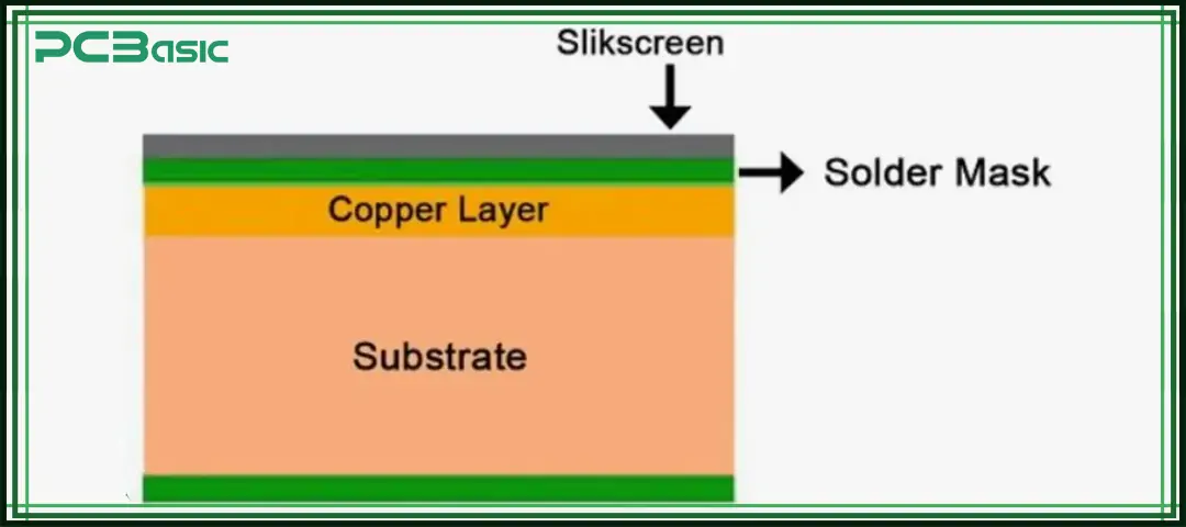
The base material or substrate, often made of fiberglass (FR4), provides mechanical rigidity to the PCB.
Depending on whether the PCB is single-sided, double-sided, or multi-layered, one or more layers of copper are laminated to the substrate. These copper layers carry the electrical currents around the board.
This protective layer, which is often green but comes in various colors, is laid over the copper to prevent accidental contact and short circuits. It also helps to protect the copper from external factors.
Usually white, this layer contains symbols, numbers, and letters that provide a reference for assembling components. It's a guide that ensures components are correctly placed and oriented.
These are shiny, gold-plated terminals seen on the edge of some PCBs. They're used to interface with other boards or devices.
These are tiny holes drilled into the PCB that enable electrical connection between the various layers of copper.
The essence of a PCB lies in its intricate design and the harmony between these foundational elements, facilitating complex electronics in compact spaces.
Crafting a Printed Circuit Board (PCB) is an intricate endeavor, necessitating meticulous precision across several pivotal phases. When executed seamlessly, these stages guarantee the board's exceptional functionality, durability, and efficiency.
The three manufacturing processes are Design, Fabrication, and Assembly.
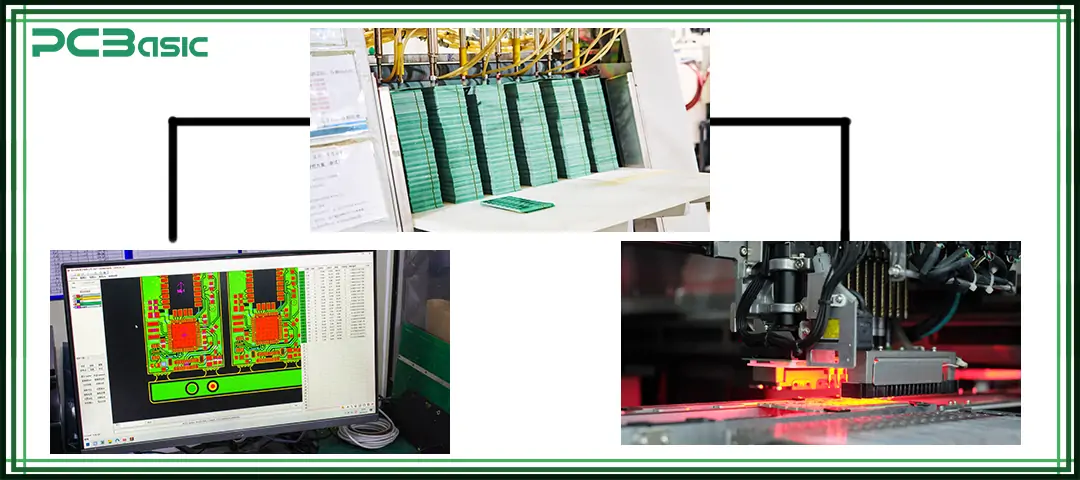
Initiating the process is the design phase, where computer-aided design (CAD) software takes center stage. Here, meticulous details such as component layout, conductive trace routing, and the strategic placement of vias and PTHs materialize.
Apart from the foundational layout, the design phase also entails discerning suitable materials, orchestrating the layer composition, and defining trace measurements, all in alignment with specific electrical and mechanical prerequisites.
Once this design reaches its fruition, it metamorphoses into manufacturing directives, notably the Gerber files, essentially guiding the subsequent fabrication phase.
Fabrication is where the virtual design translates into a tangible PCB. Typically, the journey commences with a foundational substrate graced with copper layers, like the prevalent FR-4 (a fire-retardant composite forged from woven fiberglass cloth amalgamated with an epoxy resin binder).
This copper subsequently undergoes a meticulous etching—either chemically or mechanically—to manifest the envisioned trace pattern. In multilayer PCBs, distinct layers are first individually crafted and later fused using a combination of heat and pressure.
Following the trace formation, drilling ensues, paving the way for component mounting and facilitating inter-layer connections. These freshly drilled cavities are then copper-plated, birthing PTHs or vias.
A solder mask swathes the traces as a protective measure, and a silkscreen layer, providing component cues and vital details, is layered atop. To wrap up the fabrication, the PCB undergoes treatments to stave off oxidation, ensuring its longevity.
The assembly phase brings the PCB to life as electronic components find their rightful place on the board. Primarily, there are two techniques to anchor these components: the traditional through-hole soldering and the avant-garde surface-mount technology (SMT).
The former sees components with leads embedded into the pre-drilled apertures, subsequently soldered onto the board's reverse traces. To encapsulate, each juncture of the PCB manufacturing journey demands unparalleled precision and an eye for detail.
An in-depth grasp of this meticulous procedure empowers engineers and designers, enabling them to harness insights that fine-tune performance, economize costs, and enhance the manufacturability of their PCB blueprints.
In electronics, the Printed Circuit Board Assembly (PCBA) emerges as an intricate yet cohesive work of art. But what exactly constitutes this crucial element in our devices?
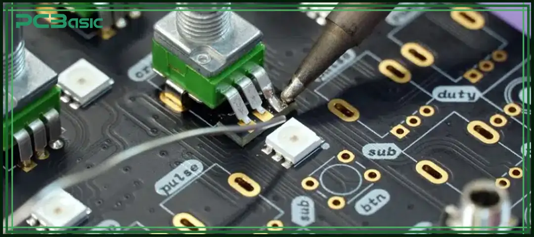
The heart of the PCBA is the Printed Circuit Board (PCB). It is the foundational platform, a canvas, if you will, upon which everything else finds its rightful place. Composed of laminate materials and often layered, the PCB provides structural rigidity while housing conductive pathways.
Elegantly adorned on this board are the diverse electronic components. These usually are from passive elements like resistors, capacitors, and inductors to active ones such as transistors and integrated circuits, and each component plays a pivotal role. These building blocks bring functionality to the board, each contributing its unique electrical characteristic.
Serving as the veins of our PCBA, the traces are thin conductive pathways, facilitating the seamless flow of electrical currents. Conversely, Vias act as bridges, connecting different layers of a multi-layered PCB, ensuring the harmony of signals throughout.
Before placing the components, a solder paste (a mixture of fine solder particles and flux) is applied to the board where the components will be attached. This ensures a solid connection when heated.
The consistent application of the paste is crucial to the assembly process, as it determines the quality of connections. The paste's composition allows for optimal electrical conductivity and mechanical strength.
A PCBA is more than just its parts; it's a harmonious collaboration of meticulously chosen and precisely placed components. Each element, while significant on its own, collectively contributes to the overarching functionality and performance, making the PCBA a marvel of modern engineering.
Assembling a Printed Circuit Board (PCB) is like bringing a schematic design to tangible life. Two dominant methodologies steer this intricate process: through-hole technology (THT) and surface-mount technology (SMT).
Emerging from the foundational years of electronics, through-hole Technology (THT) stands as a beacon of traditional PCB assembly methods.
At its core, THT is characterized by its systematic process. It involves placing extended leads of electronic components through meticulously drilled holes on a PCB.
Protracted from the opposite side, these leads are then anchored securely by soldering them to designated pads. This ensures both a mechanical and an electrical connection.
While seemingly straightforward, the entire process requires precision, especially in aligning the components' leads with the PCB's drilled holes.
THT's claim to fame lies in its unmatched resilience and endurance. Here's a more detailed exploration of some of its applications:
● Aerospace: THT is a staple in an environment where every second and every connection counts. From satellites to spacecraft, these systems cannot afford even the minutest of malfunctions. THT's robust connections ensure that vibrations or temperature variations in space don't compromise the equipment.
● Military Hardware: On the battleground, reliability is paramount. Military gear, ranging from communication devices to advanced weaponry, leans on THT for its proven track record. Its ability to withstand harsh conditions and sustain performance makes it an obvious choice.
● Industrial Machinery: In industries where machines operate incessantly, the electronics governing them face constant wear and tear. With their sturdy connections, THT assemblies ensure these machines function seamlessly, minimizing downtime.
● Vintage Electronics: THT is the go-to assembly method for enthusiasts of retro electronics and vintage radios. Not only is it historically accurate, but it also provides the longevity that such devices originally boasted.
Mapping and Design: The board is carefully mapped before drilling to ensure the drilled holes correspond with the circuit design. High-resolution X-rays or automated machines are often employed for this task.
Precision Drilling: Utilizing advanced machinery, holes are drilled into the PCB with utmost precision. These holes are designed to accommodate the leads of the components. Their diameter, depth, and location ensure a seamless assembly process.
Lead Alignment: The component leads are carefully aligned to match the drilled holes before insertion. This ensures a snug fit and facilitates subsequent soldering.
Manual vs. Automated Insertion: Depending on the complexity, scale, and required precision, components may be inserted by hand or through automated pick-and-place machines. Manual insertion might still be preferred for larger components or specialized assemblies due to the tactile feedback it provides.
Flux Application: A flux layer is applied to the area before soldering. The flux aids in the soldering process by cleaning the leads and the board, thus ensuring a stronger bond.
Wave Soldering: This is the predominant method for THT. With its protruding component leads, the PCB is passed over a cascading wave of molten solder. As the board moves, the solder adheres to the leads, ensuring a solid electrical and mechanical connection.
Cooling and Solidifying: Once the soldering is done, the board is passed through a cooling zone to allow the solder to solidify, firmly anchoring the components in place.
Trimming: The extended leads, now protruding from the opposite side of the PCB, are carefully trimmed down to a desired length using manual tools or automated cutters. This ensures a neat appearance and prevents any unintentional electrical contact.
Cleaning: Post-trimming, the board often undergoes a cleaning process to remove any residual flux or debris. This step ensures the board's longevity and optimal functionality by preventing potential corrosive damage or electrical shorts.
While methodical and intricate, the THT assembly process aims to deliver a robust and durable PCB capable of withstanding challenging environments and prolonged usage.
Surface-mount technology (SMT), which emerged as a revolutionary shift from conventional assembly methodologies, hinges on placing and soldering components directly onto a Printed Circuit Board (PCB) surface.
Unlike its through-hole predecessor, which requires leads to pass through holes, SMT leverages tiny pads for soldering, underscoring its commitment to miniaturization. This results in a reduction in board size and an enhancement in its electrical performance, especially at high frequencies.
The methodology's name is also derived from its very essence—the components are "surface-mounted" onto the PCB, enabling a dense integration of components on both sides of the board if needed.
The dexterity and scalability inherent in SMT have made it the cornerstone of modern consumer electronics. Its prowess is particularly evident in devices where form factor, weight, and performance are paramount:
● Smartphones: Almost ubiquitous today, smartphones are a testament to the capabilities of SMT. From their high-resolution screens to their multicore processors, these devices' compact and efficient nature directly results from SMT's intricate assembly techniques.
● Tablets: Bridging the gap between smartphones and laptops, tablets—with their larger screens and enhanced capabilities—also rely on SMT to maintain a slim profile without compromising performance.
● Wearables: Devices like smartwatches, fitness bands, and augmented reality glasses demand the utmost miniaturization. SMT's ability to densely populate a PCB ensures these wearables remain lightweight, versatile, and powerful.
Before the assembly process can begin in earnest, precise amounts of solder paste need to be applied to the PCB. This is achieved using a stencil, a thin sheet (often stainless steel) with holes cut in positions corresponding to solder pad locations on the PCB.
A squeegee blade then sweeps across this stencil, pressing the solder paste through the holes and onto the PCB. Ensuring accurate solder paste deposition is pivotal, as it impacts the quality of solder joints and, consequently, the performance of the assembled board.
Once the solder paste is in place, the next step is populating the PCB with components. Given the minuscule size of many modern components, this task requires a high degree of precision.
To achieve this, state-of-the-art pick-and-place machines are employed. These machines select components from feeders, verify their type and orientation, and then place them onto their designated locations on the PCB with impeccable accuracy.
After components are placed, the board is sent into a reflow oven—a specialized machine that subjects the PCB to a controlled temperature profile. Starting with a preheat phase, where the entire board is gently heated to eliminate moisture, the temperature is ramped up.
As the board navigates through the oven, the solder paste reaches its melting point, effectively "reflowing" to form solid solder joints that mechanically and electrically connect components to the PCB. Once the soldering phase is complete, a cooling phase solidifies the solder, finalizing the connections.
4. Inspection & Quality Control
Ensuring a flawless assembly process is not just about the placement and soldering of components; rigorous post-assembly inspection is paramount. Automated Optical Inspection (AOI) is a key player in this stage.
Through high-definition cameras and sophisticated software algorithms, AOI systems scan the PCB to check for potential defects—like misalignments, tombstoning, or insufficient solder. Any discrepancies detected are flagged for further review or rework, ensuring each board meets stringent quality standards before moving forward.
When we talk about PCBA testing, we refer to testing the IC programming, power, current, voltage, and circuit continuity on the processed PCBA board. Those tests strictly follow the PCBA test standard and test the circuit board points according to the customer's test plan.
PCBA testing is the most critical quality control method in the entire PCBA processing process and is a vital link to strictly controlling shipments' quality.
PCBA tests mainly include:
1. ICT Test: Test for circuit on-off, current and voltage values, fluctuation curve, amplitude, and noise.
2. FCT Test: Often referred to as functional testing. This test will run a function simulation test on the PCBA board, thereby discovering problems in hardware and software.
3. Flying Probe Test: The flying probe tester uses probes to conduct electrical tests on electronic components' value and electrical characteristics.
4. Aging Test: Uninterrupted and continuous power-on for the PCBA board that has passed the FCT test, simulate user input and output, observe whether the PCBA board will fail during long-term and periodic work, and test the durability and stability of the product.
5. Harsh Environment Test: Expose the PCBA board to extreme temperatures, humidity, splashing water, drop, and vibration, and obtain the test results of random samples to infer the reliability of the entire PCBA board batch product.
The above are the standard PCBA test methods. The operation should choose different test methods according to the actual situation of the product. A PCBA processing factory with rich testing experience can spend the least time testing your products to ensure that the products have good quality and better durability.
Printed Circuit Boards (PCB) and Printed Circuit Board Assemblies (PCBA) are intrinsically linked stages in electronics manufacturing. A PCB provides the foundational structure, consisting of conductive traces, pads, and other features etched on a non-conductive substrate.
It serves as the blueprint upon which electronic components will later be affixed. Transitioning to PCBA occurs when these electronic components— like resistors, capacitors, and integrated circuits—are mounted and soldered onto the PCB, making it a complete, functional circuit.
In essence, while a PCB is like an empty canvas, a PCBA is the finished painting, with all components in place, ready to execute its electronic functions. Understanding the distinction and relationship between PCB and PCBA is fundamental to grasping the electronics production process.
So, when exactly should you choose between PCB and PCBA?
Selecting a PCB without the components assembled is ideal during the initial stages of product design and prototyping. A standalone PCB is sufficient when you're in the testing phase, refining the board layout, or evaluating the conductive pathways. It provides flexibility, allowing for alterations without wasting components.
Furthermore, if you have the capability and desire to handle component procurement and assembly in-house or through another specialized service, then procuring just the PCB is the way to go.
When you're looking for a fully operational board to directly integrate into a product, PCBA is the optimal choice. It is a time-saving solution, especially for mass production, as the board comes complete with all necessary components already assembled.
This ensures consistency, reduces assembly errors, and can be more cost-effective at scale. For finished products or near-final prototypes, PCBA provides a plug-and-play solution.
For some minutes now, we've been talking about PCB and PCBA, and I think it makes a lot of sense to know the application of both, don't you agree?
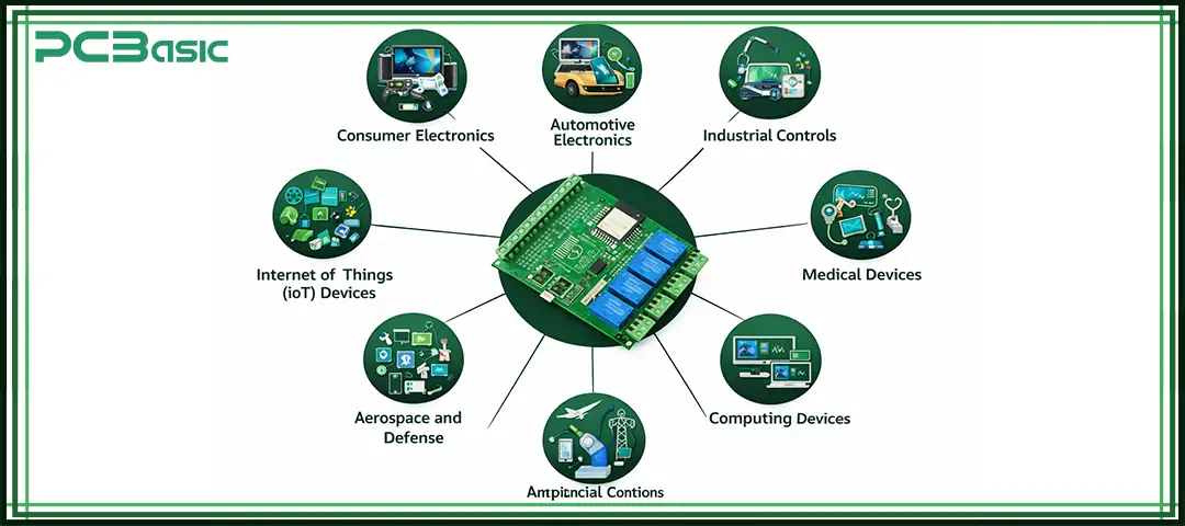
At the core of daily technologies—from the ubiquitous smartphone to the immersive experience of modern televisions—lie PCBA vs PCB. They serve as the operational foundation, bridging microprocessors, memory modules, and other pivotal components.
In the evolving transportation landscape, especially with the rise of electric vehicles (EVs), PCB and PCBA have become indispensable. They govern battery management, enhance energy utilization, and empower autonomous navigation. As we veer towards a more electrified future, the significance of these boards in ensuring vehicular efficiency and safety cannot be overstated.
Within industrial arenas, PCBs and PCBAs animate the heart of machinery, from the decisive programmable logic controllers (PLCs) to dynamic motor drives and nuanced sensors. Their presence guarantees seamless operational flow.
In medicine, accuracy is paramount. Be it a simple heart rate monitor, the workings of an MRI scanner, or the precision of robotic surgical instruments, the unwavering reliability of PCB vs PCBA is a prerequisite.
Whether in expansive servers or personal laptops, computing prowess is bolstered by meticulously crafted PCBAs. These boards host many essential components, such as CPUs, GPUs, and RAM, forming the crux of computational strength.
The digital threads that connect us, manifesting as cellular networks or vast internet channels, stem from high-caliber PCBAs. These underpin the efficacy of routers, switches, and expansive base stations.
The demands on technology are immense in the rigorous spheres of aerospace and defense. Here, PCBA and PCB adhere to stringent criteria and anchor many applications, from intricate cockpit instrumentation to astute missile guidance systems.
As we usher in the age of IoT, marked by interconnected smart homes, wearable technology, and industrial sensors, the compact yet potent PCBAs stand as the silent enablers.
At PCBasic, our primary focus is delivering top-tier intelligent manufacturing solutions tailored for small and large-scale PCBA productions. As a PCB design and fabrication leader, we pride ourselves on being more than just a PCB company.
We're your partner for:
● Intelligent PCB Manufacturing
● PCB Design
● PCB Fabrication
● R&D Solutions
● Material Selection
● Integrated Management Systems
● Surface Mount Technology (SMT)
● Through-Hole Assembly
● BGA X-Ray Inspection
● Prototype PCB Assembly
● PCB Testing
We stand by our commitment to swift service without compromising on quality. With our expertise in PCBA technology and PCB design services, our clients can trust us to deliver innovative R&D solutions and reasonable material selection, ensuring optimal results for OEM order production.
Our proprietary management systems, including CRM, MES, ERP, and IoT, have been meticulously developed in-house. This forward-thinking approach allows us to excel in digital intelligence, setting us apart as an industry front-runner.
We have garnered a wealth of knowledge and proficiency in serving diverse sectors such as industrial control, smart home ecosystems, advanced instrumentation, vehicle IoT, communication power infrastructure, medical device technology, automotive electronics, and aviation.
Moreover, our commitment to ensuring functionality is unwavering, evident in our rigorous Prototype PCB Assembly and PCB Testing protocols.
So, when you partner with us, you're aligning with a team that prioritizes your objectives, ensuring a seamless journey from design to delivery.

Assembly Enquiry
Instant Quote
Phone contact

+86-755-27218592
In addition, we've prepared a Help Center. We recommend checking it before reaching out, as your question and its answer may already be clearly explained there.
Wechat Support

In addition, we've prepared a Help Center. We recommend checking it before reaching out, as your question and its answer may already be clearly explained there.
WhatsApp Support

In addition, we've prepared a Help Center. We recommend checking it before reaching out, as your question and its answer may already be clearly explained there.