
Global high-mix volume high-speed PCBA manufacturer
9:00 -18:00, Mon. - Fri. (GMT+8)
9:00 -12:00, Sat. (GMT+8)
(Except Chinese public holidays)





HomePage > Blog > Knowledge Base > AI Vision PCBA for Reliable Image Processing Hardware
Table of Contents
1. A Vision Board Is a Data Path, Not One PCB
2. Match Inspection to What the Board Can Hide
3. Test the Image Path Under Real Operating Conditions
4. Make the First Build Explainable Before It Scales
5. Conclusion
6. FAQs
If the AI vision board can produce accurate images in the laboratory, does that mean it will also be stable during mass production? Not necessarily.
Sensor data needs to pass through processor, memory and high-speed interface, meanwhile, the power supple should keep stable under operating load. If any one of these steps fails, the final image result may be affected. Some problems are hidden beneath BGA and other packaging, and they are difficult to detect through visual inspection alone.
How should these risks be identified during production? The key point is not to conduct all the tests. Before production, we need to know which areas have higher risks, how to control during the production process, and finally how to verify. The problems solved by SPI, AOI, X-Ray and functional testing are not the same. For AI vision PCBA, the completion of the mounting process is only the first step. What really needs to be confirmed is whether the entire board can complete its task stably.
On an image processing board, different parts may have problems in different ways. The connections of the camera or sensor connectors need to be stable both mechanically and electrically. If the processor or accelerator is packaged in BGA, the solder joints below are difficult to be seen from the outside. The stability of actual data transfer should be examined in addition to connectivity in the memory and high-speed connectors. The same is true for the power supply; just because it functions normally when there is no load does not guaranty that it won't have issues when in use.
Before the build starts, you can first sort out the whole data path from input to output. See how the data enters the processor from the camera or sensor interface, travels thru the memory and other interfaces, and then outputs the image or processing results. A lot of projects miss some details here. Like, the BGA package is already determined, but the image format, cable connection, data rate, and even the actual operating temperature and load conditions aren't specified in advance.
|
Board area |
Possible problem |
What to check |
Information needed |
|
Camera or sensor input |
Reversed connector, enclosure stress, or failure during image transfer |
Orientation, placement, and input-interface check |
Connector drawing, cable route, mating part, input format, fixture access |
|
BGA processor or accelerator |
Hidden solder defects, voids, bridging, or abnormal joints |
Package review, SPI, reflow control, X-ray, and functional test |
Package data, ball map, approved part, thermal limits, interface tests |
|
Memory and data interface |
Powers up normally but loses data under real traffic |
Functional test with target data flow and error limits |
Memory setup, data rate, test pattern, pass/fail criteria |
|
Power and output stage |
Stable at idle but fails under load |
Functional test under expected load |
Input range, load states, peripherals, output protocol, acceptance limits |
This table cannot replace design validation, but it can help the production team better understand what needs to be checked. If you provide only the BOM and basic assembly requirements, the supplier may know how to attached the components, but they won’t know which functions require focused verification. Instead of simply stating “conduct PCBA testing”, it would be better to directly specify which connectors need to be tested, which BGA components require X-Ray inspection, and which image data path needs to be run under actual load.
Different problems require different detection methods. In high-density SMT assembly, SPI can detect problems related to solder paste printing before reflow soldering, while AOI can check the position, polarity of components, and some visible welding issues, but they cannot see the solder joints beneath BGA. If the board uses BGA or other hidden solder joint packaging, X-Ray inspection needs to be added. And it should not simply be written as "check BGA", but the inspection standards should be set according to the specific packaging and possible problems.
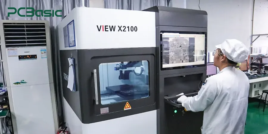
The BGA inspection is the same. The visual inspection can check if the components are properly mounted and if the positions are correct, but it cannot reveal the solder joints beneath the package, nor can it guarantee that these solder joints will be reliable in actual operation. Therefore, it is best to clearly state in the production materials which BGA components need to be inspected, what X-Ray focuses on, and under what circumstances rework is required. This way, production staff and quality personnel will be able to more easily understand how to conduct the inspection, rather than just seeing the phrase "inspect BGA".
If you’re comparing the BGA assembly capabilities of a supplier, you should not only consider whether it has X-ray or AOI equipment. Take PCBasic as an example, we will conduct pre-production process evaluations, BGA storage, necessary baking, as well as SPI, AOI, X-Ray, fixture preparation and functional testing in BGA assembly. However, these steps are not simply following a routine process; they need to be arranged based on the specific BGA packaging, test inputs, and in accordance with standards. For you, what is more important to focus on is: Can the factory continue from packaging inspection to overall board functional verification? For image processing hardware, both of these aspects are very important.
If you want to learn more about how X-Ray examines BGA solder joints and internal defects, you can refer to the X-Ray inspection introduction provided by PCBasic. In actual production, X-Ray does not inspect all the components on the entire board in the same way. Instead, it decides which parts to focus on based on the specific packaging, location, and risks.
However, there is one thing to note: X-Ray can detect problems with hidden solder joints, but it cannot tell you whether the camera data has been correctly decoded, whether the processor can complete the actual tasks, or whether the external interfaces are stable during continuous operation. These issues cannot be confirmed solely by X-Ray; rather, they need to be verified through subsequent functional tests.
Just making sure the board can turn on normally is insufficient for image hardware. Additionally, you must determine whether it can function steadily in an actual workplace. To enable the processor to carry out the necessary activities, you can first connect a known sensor or camera. Then, you can verify that the photos, data, output results, or interface answers are normal. During the test, you should also consider the real power supply and peripheral device loads. We usually do not consider "able to power on" as the completion of the test because a board being able to start does not mean it can stably complete image processing when actually working.
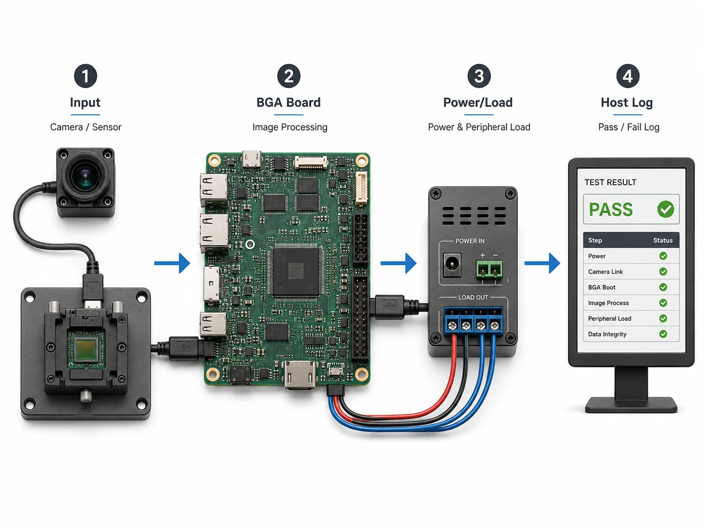
At this point, the PCBA testing truly becomes meaningful. You need to clearly state the testing conditions first, such as what input sources to use, what images or data to test, how to connect the cables and connectors, what the power supply range is, and what constitutes a pass. If the board is also to be connected to a camera, display, storage device, or host, it is also advisable to include the specifications of these devices and communication requirements. In this way, when real problems occur, we can try to restore the testing state at that time as accurately as possible, rather than just taking a board and guessing how it was tested before.
This can also avoid another common problem: using one inspection method to determine a problem that cannot be seen in the first place. SPI and AOI are suitable for checking what they can directly see. BGA and other hidden solder joints can be inspected using X-Ray, while data transmission and actual functions require functional testing to confirm. You don't need one device to prove all the problems; instead, the combination of different detection methods is more effective.
If you want to have a more intuitive understanding of BGA X-Ray testing, you can refer to the BGA X-Ray demonstration provided by PCBasic. Such testing results can be used as part of the quality assessment and subsequent traceability, but it still cannot replace the full board functional verification. For AI visual boards, ultimately, the cameras, processors, and output ports need to be activated to confirm that the entire data path can operate normally under actual working conditions.
After the first board has passed the test, the more important question is: Can we clearly explain why it passed? What materials were used, which processes were followed, what inspections were conducted, and under what conditions was it passed the functional test? All this information needs to be retained. Therefore, before using the trial production board as a reference for subsequent production, it is best to fix the PCB version, BOM, substitute materials, BGA packaging information, screen or mounting requirements, first article standards, and test records first.
For this type of AI vision board, this is particularly important because there are usually multiple sensors and interfaces connected around the processor. The detection results of the BGA should be saved together with the conditions used for the entire board testing at that time. If problems arise later, the reason might simply be the replacement of substitute materials, adjustment of a certain process parameter, change in connector configuration, or differences in test conditions compared to before. If these information is not recorded clearly, the team may repeatedly test the same board but still be unable to determine which change affected the result.
Once the engineering documents have clearly stated the inspection requirements, PCBasic can use MES to link up records like IQC, first-piece inspection, process inspection, and functional testing. This way, if there's a problem later, it'll be easier for us to look back and check whether it's because the materials have changed, the process conditions have changed, or the testing conditions are different from before. Of course, these records can't replace the info the customer needs to provide, like actual image input, workload, BGA packaging list, and acceptance criteria.
When you're making an inquiry, you'd better get ready Gerber and stack-up, BOM and approved alternative materials, BGA package list, assembly drawing, camera or sensor interface instructions, power supply information, devices to be connected, and the functional test conditions of the image path all together. The clearer the materials are, the easier it'll be for the production team to know exactly how to assemble this board and which parts need key verification. Instead of waiting until the production plan's set and then thinking about what tests to do on the fly.
For an AI vision board, the completion of component mounting is just the beginning. What truly matters is ensuring that the image data can be properly input, processed, and output, whether the key positions such as BGA have been correctly inspected, and whether the entire board can operate stably under actual load. By thinking these issues through in advance, the subsequent testing and inspection processes will not become a simple "doing each one separately".
If you are preparing an AI vision PCBA project, you can first organize the Gerber files, BOM, substitute materials, BGA packaging information, interface descriptions, power conditions, and functional test requirements. The PCBasic electronics manufacturing team can help check the BGA assembly plan, X-Ray inspection, and functional test requirements before the quotation. After preparing the materials, you can submit the project through the engineering review form.
Q1: What should an AI vision PCBA package include before manufacturing?
A1: Include the PCB revision and Gerbers, BOM and approved alternates, BGA package information, assembly drawing, connector and cable details, sensor or camera input definition, power/load conditions, connected devices, and written functional pass/fail criteria. The key is to describe the complete input-to-output path, not only the component list.
Q2: When does an image-processing board need X-ray inspection?
A2: X-ray is appropriate when the board uses BGA or other packages with solder joints that cannot be evaluated visually. In a PCB assembly BGA review, specify the affected package references and inspection criteria. X-ray verifies hidden-joint conditions; it should be combined with functional verification when the board must process image data or communicate with another device.
Q3: What should functional testing record for PCBA testing?
A3: Record the board revision, test fixture or connected equipment, input source, operating supply and load, image or data pattern, expected output, measured result, pass/fail limit, and the operator or system record. This makes a later failure reproducible and gives engineering a basis for comparing the first article with later builds.
Assembly Enquiry
Instant Quote


Phone contact

+86-755-27218592
In addition, we've prepared a Help Center. We recommend checking it before reaching out, as your question and its answer may already be clearly explained there.
Wechat Support

In addition, we've prepared a Help Center. We recommend checking it before reaching out, as your question and its answer may already be clearly explained there.
WhatsApp Support

In addition, we've prepared a Help Center. We recommend checking it before reaching out, as your question and its answer may already be clearly explained there.
