Due to technological advancements, PCB design for small and complex chips has experienced a huge rise in demand. Hence, working with a packaging method that accommodates these high I/O density chips while ensuring cost-effectiveness is important. This is where BGA plays an important role.
In this article, you will understand what BGA assembly is, its pros and cons, and the challenges faced during assembly. We will also explain how to check the quality of solder joints. Please read on as we explain the topic further.
What is BGA Assembly?
There is a need to understand what BGA is before venturing into what BGA assembly is all about.
About PCBasic
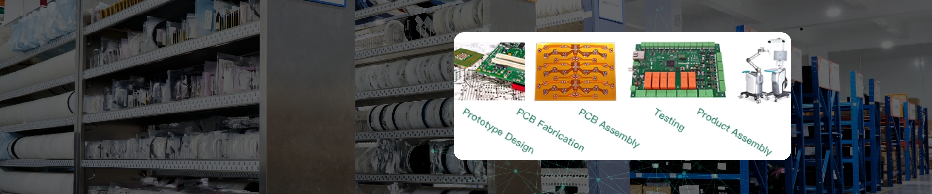
Time is money in your projects – and PCBasic gets it. PCBasic is the pcb assembly company that delivers fast, flawless results every time. Our comprehensive PCB Assembly Services include expert engineering support at every step, ensuring top quality in every board. As a leading PCB Assembly Manufacturer, we provide a one-stop solution that streamlines your supply chain. Partner with our advanced PCB Prototype Factory for quick turnarounds and superior results you can trust.
So what is BGA?
BGA(Ball Grid Array)is an integrated circuit package (IC package) in which the electrical connection is achieved by arranging small solderingballs in a grid pattern. This type of packaging is primarily used for high-density applications and offers significant improvements over traditional packaging methods such as perforated packaging or surface mount components (SMD).
In BGA packages, the traditional pins are replaced by small solder balls that are arranged in a matrix or grid at the bottom of the element. These solderingballs connect the BGA chip to the PCB through a process called ball grid array soldering. BGA components are widely used in high-speed and high-power applications that require advanced thermal management and electrical performance.
BGA Assembly
BGA assembly refers to the process of mounting ball grid array (BGA) components onto a printed circuit board (PCB) through a technique called ball grid array soldering. Instead of using pins in traditional integrated circuit packages, BGA uses welded balls arranged at the bottom of the component that act as an electrical connection between the BGA chip and the PCB, providing efficient data transmission and power supply.
PCBA manufacturers use BGA assembly to mount devices with hundreds of pins. Unlike traditional SMD packaging, BGA assembly uses an automated process, which means that the solderingprocess requires precise control. By using a thermal enhancement mechanism to reduce resistance, BGA assembly provides better thermal performance and more stable electrical connections than traditional packaging methods.
In addition, BGA assembly has obvious advantages in terms of functional capabilities. The high-density design of the BGA assembly makes it ideal for integrated circuits that require high-speed and high-power processing.Especially for those applications that require high thermal management and electrical performance, such as high-frequency processors and memory chips, BGA assembly is the ideal.
Next, we will delve into the advantages of BGA assembly over traditional packaging methods and its application in modern electronics.
Advantages of BGA assembly
Below are the benefits of BGA assembly.
Increase in density
BGA assembly involves the use of more solder balls. This causes an increase in the connection between these balls. The connection leads to an increase in the density of connections. Also, these numerous solder balls present reduce the space available on the circuit board. This leads to lighter and smaller products.
Better electrical performance
BGA assembly offers better electrical performance. This quality is due to the shorter path between the circuit board and the die. BGA assembly dissipates heat often due to its tiny size. Also, this package lacks pins, which can easily bend and break, increasing its electrical performance and stability.
Improved heat dissipation
BGA assembly ensures improved heat dissipation. It possesses this quality due to its low thermal resistance and tiny size.
Self-alignment
Through BGA assembly, the PCB space is well utilized. This is because the soldering balls usually self-align underneath the board. BGA assembly ensures the use of the entire circuit board.
What are the Steps Involved in BGA Assembly?
The process of BGA assembly deals with the mounting and soldering the BGA components on PCBs. Here are the steps:
PCB Design and Preparation
This step involves preparing printed circuit boards. The process is possible by applying solder paste to pads where the BGA soldering will happen. The solder paste comprises flux and solder alloy, which aids in soldering.
Solder Paste Printing
This step involves the application of solder paste on the PCB metal pads through stencil printing. The stencil’s thickness helps determine the quantity of solder paste to use. Utilize laser-cut stencils to ensure a uniform solder paste transfer to the PCB.
Components Placement
BGA components are usually more easily mounted than QFP components, which have a pitch of 0.5 mm. The physical characteristics of BGA components cause them to have high manufacturability.
This step is also called the “Pick-and-place” step. The process describes how an automated machine picks and places the BGA components on the printed circuit boards. The machines usually rely on high-quality cameras. This is to ensure the accurate placement of the components.
Reflow Soldering
Here, a reflow oven helps to heat the board. The reflow oven melts the solder paste. This causes a strong bond between the circuit board and the BGA components. Also, small metallic balls underneath the BGA components melt inside the solder joints.
Inspection and Testing
Inspection is important to ensure that the BGA components are properly fixed. Also, there shouldn’t be defects like shorts, open connections, etc. Due to the physical structures of the BGA components, visual inspection won’t work. Therefore, an X-ray inspection helps to check soldering defects. These defects include short circuits, voids, air holes, and more. Then, the electrical tests help to find defects like short and open circuits.
How to ensure good soldering in BGA assembly?
Ensuring good solderingin BGA assembly is key to ensuring the performance and reliability of BGA PCB assembly. So how do you ensure that solderingis OK during BGA assembly? Here are some best practices from years of experience that can help you achieve good solderingin your BGA assembly:
1. The first step to ensuring good solderingstarts with a good BGA PCB design. When designing BGA PCBs, you need ensure proper pad design, good thermal management, and ball spacing. Also, the width and spacing of the wires on the pad must be designed well, which is essential for reliable soldering.
2. Use high quality solder paste and apply appropriate amount of solder paste to avoid excessive or insufficient solder paste. In the BGA assembly process, the solder paste is coated on the PCB pad through the template, so the steel mesh template must be accurate. Only accurate and consistent solder paste coating can achieve good solder joints.
3. Precise control of the temperature curve to avoid overheating or underheating resulting in defects such as cold welding spots.
4. After the BGA PCB is assembled, use X-ray equipment to check whether there are cold welding spots, pores, Bridges and other defects; Use electrical testing to identify short or open circuit problems. Because solder joints are often hidden under BGA components, problems cannot be fully detected by visual inspection alone.
5. Choosing a reputable BGA assembly supplier is crucial. BGA assembly suppliers with experience in handling complex assemblies are able to ensure that the process meets a high standard. Choosing a BGA PCB assembly supplier that specializes in BGA assembly services ensures higher assembly quality.
6. The BGA assembly process should be carried out in a controlled environment to prevent contamination such as dust or moisture that could affect the quality of the welding.
Challenges Faced During BGA assembly
Although BGA assembly offers many benefits, it comes with challenges. Below are some challenges faced during BGA assembly.
Soldering Defects
The soldering process isn’t easy, and even the use of machines isn’t accurate. Therefore, it is possible to face soldering defects during BGA assembly. These defects include excessive soldering, openings, solder bridges, component shifting, etc.
Repair and Rework
Repair and rework tasks on BGA Assemblies are usually challenging. This is because of its dense components. Also, there is a need for specialized skills and tools.
Inspection Limitations
The BGA assembly is always very close to the solder balls. This makes it very challenging to perform an inspection on the package.
Time-Consuming Process
The process of BGA assembly could be time-consuming. This is because the engineer must properly attach the components to the board before soldering.
How to Check the Quality of Your Solder Joint
Solder joints are very complex and have irregular shapes. Therefore, checking the quality by visual inspection would take time and effort. Thus, for more complex issues, it’s advisable to use X-ray imaging. Let us consider both methods.
Visual Inspection (Optical Inspection)
This method for checking solder joint quality is only effective for detecting defects. These include closed circuits, the absence of solder in joints, and more. The method is straightforward because you only need the naked eye to inspect.
X-ray Inspection
This method detects bridging, incomplete wiring, voiding, and other defects. Also, it can detect majority of defects on leads and pads. This method involves inspecting the solder joints using an X-ray device. The X-ray machine is composed of the X-ray source and detector. Both are connected to the system and used to transfer the image to a screen. X-ray inspection is fast and automated, thereby saving time.
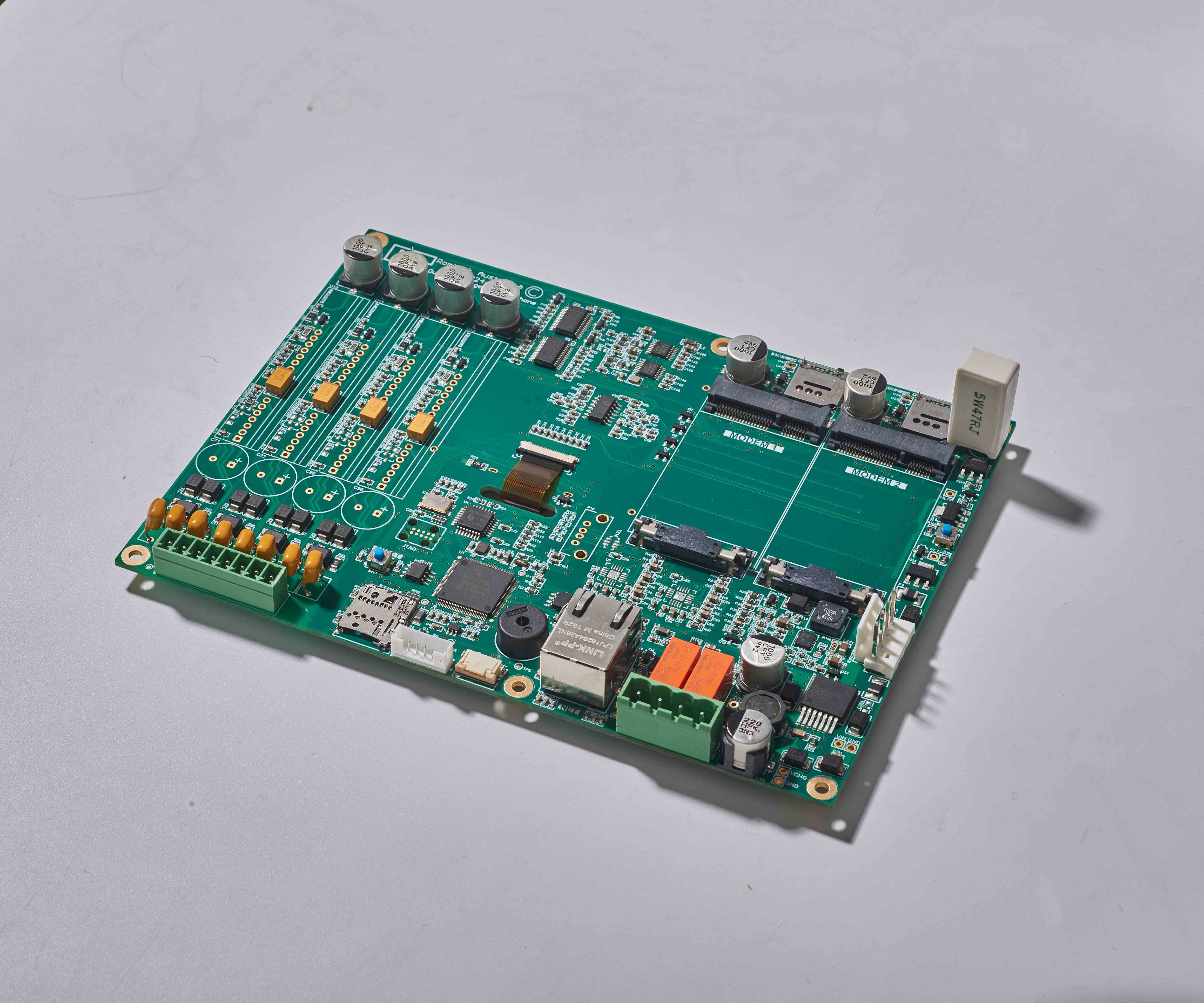
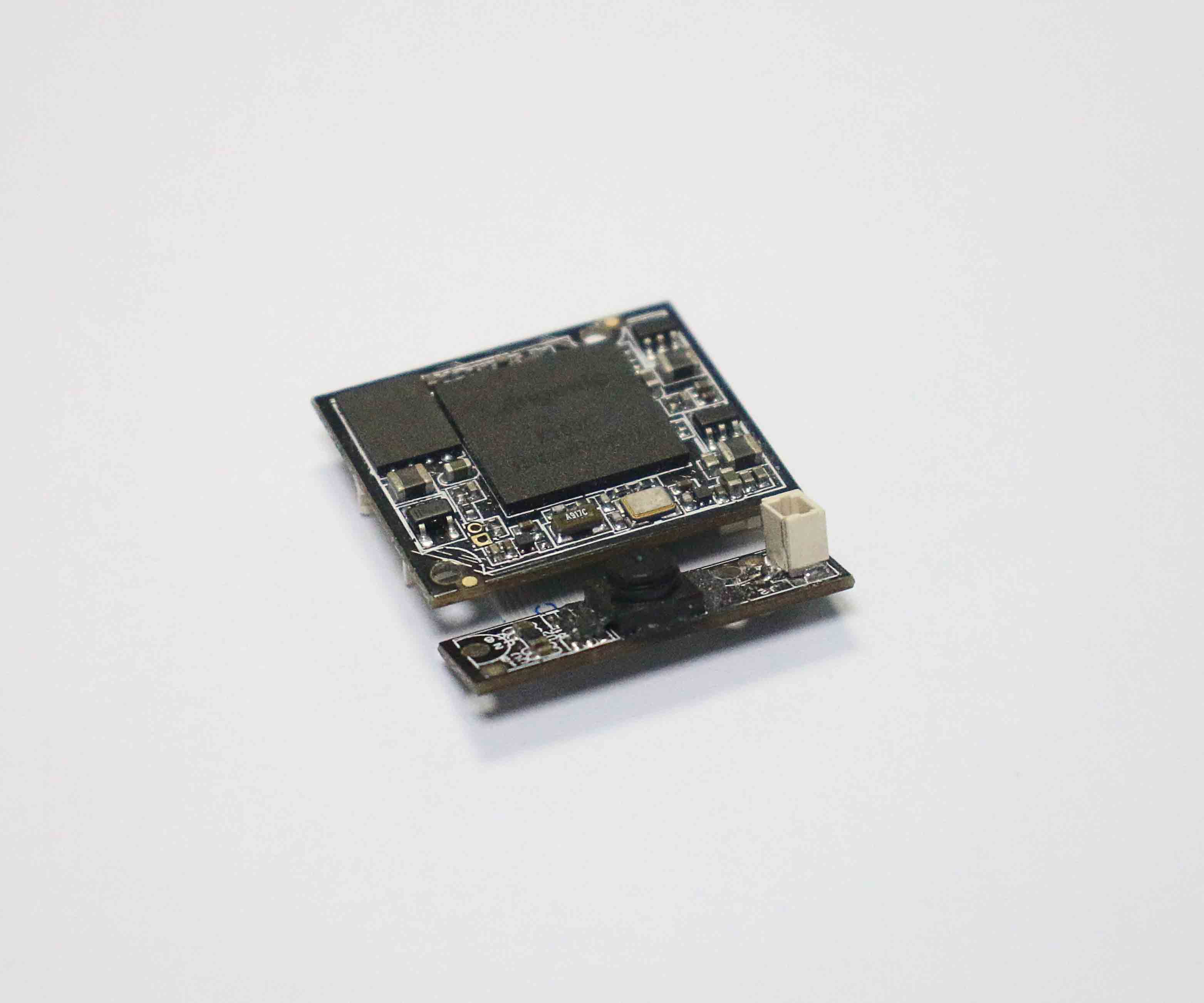
PCBasic’s Reliable BGA Assembly Services
There are many sub-categories of PCB assembly, such as layered layers: single-sided, double-sided, and multi-layer circuit boards; material properties: FPC, PCB, FPCB. Thus, when you choose a PCB assembly manufacturer for your project, you need to have a deep understanding of the characteristics of the project to know which points need special attention to pick the most suitable pcb assembly manufacturer.
BGA assembly professional factory, PCBasic provides you with turnkey BGA assembly Services.
Conclusion
BGA assembly is necessary for different industries. This is because of its reliability, effectiveness, and efficiency. Today, BGA assembly has become an important advancement in technology. There could be soldering defects, and the process could be time-consuming. Yet, BGA assembly offers many benefits. These include better electrical performance, increased density, and improved heat dissipation.
PCBasic provides one-stop BGA assembly services, including
component procurement, BGA assembly, BGA testing, functional testing, and BGA
rework. We can help your project, manufacture high-quality BGA boards, and provide
customizable PCBA solutions according
1.Fill in the product specifications according to your
2. Upload Gerber files and Bom table and other related documents
3. Get a quote in minutes and place an order quickly
How to get BGA assembly quotation?
What are the characteristics of BGA?On the back of the BGA printed substrate, spherical bumps are made in an array
manner to replace pins. The spherical bumps are solder balls, which serve as the
connection interface between the packaged IC and the PCB. BGA is a
high-performance, small size, lightweight IC package. Compared with other
packaging technologies, BGA can accommodate more pins.
What are the advantages of BGA?Compared with the previous packaging technology, the thickness and weight are
reduced; the parasitic parameters are reduced, the signal transmission delay is
small, and the frequency of use is improved; the assembly can be coplanar
welding, with high reliability, excellent heat dissipation capacity, electrical
characteristics, and high-efficiency system. Product compatibility.
Where are BGA PCBs used?
Due to the numerous advantages of BGA,
BGA PCBs are widely used
in:
CPU of mobile phones, tablets, computers and other
CPU of mobile phones, tablets, computers and other
CPU of mobile phones, tablets, computers and other
How to guarantee the quality of BGA Assembly?
1
Professional engineers will review the order, conduct process evaluation and
program production.
2
Store BGA at low temperature, bake before going online and standardize operations
3
Complete process capability, sophisticated BGA placement machine
4
Professional PCBA inspection services, such as SPI, AOI, X-Ray, etc.
5
Fixture production and functional testing
6
Fastest delivery time of 3-5 days
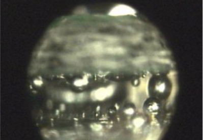
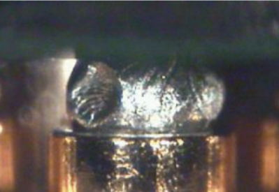
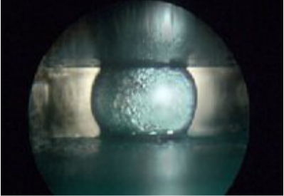
Detection of bga
The biggest disadvantage of BGA is that the solder joints after soldering are invisible,
which makes it difficult to ensure the quality and service life of the product.
The naked eye cannot directly see the solder joints of the BGA, and even AOI cannot
detect the soldering of the BGA. PCBasic uses X-Ray testing equipment to detect BGA
welding conditions and arranges IPQC to conduct random inspections at a rate of 10%
every hour.
Using X-RAY to detect BGA can detect cold soldering, incomplete melting of solder balls,
displacement, tin connection and other defects.
Why PCBasic?
1 Brick-and-mortar factory, no middleman, with more than 200 employees
2 Sophisticated production equipment such as placement machine, high-temperature
furnace, AOI, SPI, X-Ray, etc.
3 Intelligent quality control system, strict quality control
4 One-stop service, single manufacturing team, 100% privacy
We are a manufacturer with 15 years of experience in PCB assembly, we have many
efficient component suppliers, which guarantees that you will get the best quotation
and the best quality products.
Click the message box on the right to contact us now to get your custom BGA PCB
quotation, or use BGA Assembly to make an independent quotation.
What do we need in order to give you a quick quote?
Gerber
Top, Bottom, Soldermask Top/Bottom, Assembly Top/Bottom,
Silkscreen Top/Bottom, etc.
Bom
Bit No. Model Specification Package, etc.
Certification
Has passed ISO: 9001 quality certification to ensure that our products meet
industry standards,
At PCBasic, our rich BGA assembly experience and professional SMT assembly line,
as well as standardized assembly services, can place BGA components with a pitch
of 0.2MM for you.
PCBasic focuses on providing Turnkey BGA Assembly services for small and medium-sized
enterprises. What large companies are unwilling to do and what small companies
cannot do well is what PCBasic focuses on.
For more detailed BGA knowledge and other PCB related knowledge, please click here
Shenzhen low volume PCB manufacturer provides fast PCB assembly services 24 hours a day to meet the needs of customers for expedited proofing or small batch PCB assembly.
Choosing a suitable large volum PCBA manufacturer can improve product performance, PCBasic guarantees high batch PCBA projects to carry out mass production of pcba while ensuring product quality and delivery. Contact us now to get a High volume PCBA quotation.
Explore the world of Through Hole PCB Assembly with our comprehensive guide. Dive into the techniques, advantages, and applications of Through Hole technology in PCB assembly.
We use cookies to enhance your experience, analyze traffic, and provide personalized content. By clicking “Accept Cookies”, you agree to our Cookie and Privacy Policy.
Preferences
Manage Cookie Preferences
We use cookies to enhance your browsing experience. Please review the details of each cookie category below and choose your preferences.
Strictly Necessary Cookies
These cookies are essential for the website to function properly and cannot be disabled. They are typically set in response to actions you take, such as logging in or adding items to your shopping cart.
Performance Cookies
These cookies help us understand how visitors interact with our website by collecting information about traffic and usage. This allows us to measure and improve the website’s performance.
Functional Cookies
These cookies remember your preferences, such as username, language, or region, to provide a more personalized and enhanced experience.
In addition, we've prepared a Help Center.
We recommend checking it before reaching out, as your question and its
answer may already be clearly explained there.
✖
Wechat Support
In addition, we've prepared a Help Center.
We recommend checking it before reaching out, as your question and its
answer may already be clearly explained there.
✖
WhatsApp Support
In addition, we've prepared a Help Center.
We recommend checking it before reaching out, as your question and its
answer may already be clearly explained there.