Global high-mix volume high-speed PCBA manufacturer
9:00 -18:00, Mon. - Fri. (GMT+8)
9:00 -12:00, Sat. (GMT+8)
(Except Chinese public holidays)
Global high-mix volume high-speed PCBA manufacturer
9:00 -18:00, Mon. - Fri. (GMT+8)
9:00 -12:00, Sat. (GMT+8)
(Except Chinese public holidays)
Before ordering a complete set of PCBA productions, you should ensure that the PCB design layout works perfectly and manufacture a rapid PCB prototyping. To speed up a product listing and mass production, you need a trusted partner to create a PCB prototype of the circuit board and test its function.
From this article, you will understand what it needs so that you know what to expect and can provide the necessary information at any time. So what exactly do rapid PCB prototyping service and PCB layout design include?
PCBasic is a pioneer in PCB layout design, rapid PCB prototyping service and prototype PCB fabrication flied. We have the experience in PCB prototype service for over 10 years. With quick turn PCB prototypes board and layout design service teams, Our PCB prototype talent base is recognized in the PCB industry and among global customers.
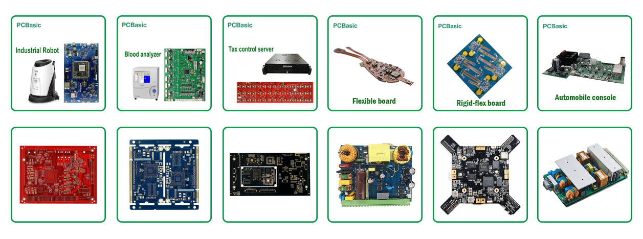
1. Custom 4 layer PCB prototype, aluminum PCB prototyping, flexible pcb prototype, rigid flex pcb prototype, and more for all your project requirements.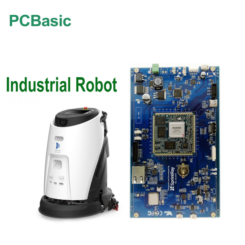
7. Designed to meet the quality, delivery, economy and any other demanding requirements of customers in different industries.
For new projects or new designs of original projects, it’s important for them that rapid PCB prototyping service meets high-quality standards and your fast PCB prototype technical specifications. If the original project is mature, you may not need the PCB prototype and PCB layout design for manufacturing.
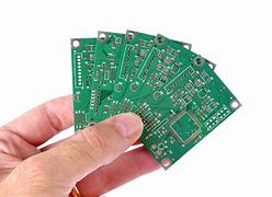
To precision layout design and high-accuracy PCB prototype, you need to submit some information about your fast PCB prototype design. The more detailed information the better. Generally, the information you provide includes the following items:
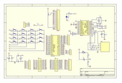
The schematic diagram is a diagram that shows the connection principle between devices on the PCB prototyping board. The schematic diagram plays an indispensable role in the process of product debugging, maintenance and improvement.
The extension from the schematic diagram will involve the rapid PCB prototyping layout design. Of course, this kind of layout is made based on a schematic diagram. By analyzing the schematic diagram and limiting other conditions of the PCB prototyping board, designers can determine the location of electronic components and the number of layers of the PCB prototyping board.
This schematic diagram is part of the initial design stage. After the completion of the first schematic diagram, PCBasic will initially check the potential defects and correct any defects that appear. Then, you can use a special PCB design tool to simulate to ensure that the rapid PCB prototyping board functions properly and as a more in-depth design check. Then we complete the first step of rapid PCB prototyping board.
BOM(Bill of Material) is a document that describes the structure of prototype PCB assembly electronic components in data format, and it is the detailed information that PCBA manufacturers buy the correct parts.
The BOM includes important information about each component, the following:
After the Engineers complete the BOM and schematic diagram of rapid PCB prototyping board layout design, PCBasic will check the documents and Confirm with the customer again. This is the second step of rapid PCB prototyping board.
According to PCBasic design specifications, design instructions, customer design requirements, and relevant checklists, our engineers connect the electronic components of rapid PCB prototyping board by routing. In our rapid PCB prototyping layout service, PCBasic analyzes signal integrity and evaluates electrical limitations to ensure the safety of board-level architecture. For complex layouts, PCBasic incorporates various simulations into our custom rapid PCB prototyping board design services.
Before the rapid PCB prototyping board is manufactured, PCBasic confirms PCB prototype files with customers, including schematic, BOM, and layout. Once our rapid PCB prototyping design layout is approved for production, we will export it to the format for prototype PCB fabrication service--Gerber file. It is used to describe the design requirements of each image of PCB prototyping board.
Gerber format is a set of document formats for PCB industry software to describe rapid PCB prototyping board (circuit layer, solder resist layer, character layer, etc.) images and drilling and milling data. Gerber has three formats: Gerber X2, the latest Gerber format, RS-274X (extended Gerber format), and old-fashioned RS-274-D. Gerber format was originally developed by Gerber company and now belongs to Ucamco. Gerber format is the standard format for image conversion in the PCB industry.
Gerber documents are usually produced by PCB prototype designers using professional Electronic Design Automation (EDA) or CAD software. Gerber documents are sent to the PCB factory and imported into CAM software to provide data for every rapid PCB prototyping service process. Gerber data can also be used to provide image data for specific equipment, such as automated optical inspection equipment, and can also be used to describe drilling information. However, the drilling data is usually in Excellon format.
|
Creating the Photo Film |
create a photo film of rapid PCB prototyping board for each layer and solder mask of the prototype PCB board. |
|
Printing the Inner layers |
apply copper to substrate material by photoresist |
|
Aligning the Layers |
align all the layers and punch accurate registration holes |
|
Fusing the Layers Together |
Stack the substrate layer, copper sheet, prepreg, aluminum foil, and copper pressing plate in sequence. |
|
Drilling the Holes |
Drill holes in the stack, which we will use later when adding components. |
|
Copper Plating |
A chemical bath was used to cover the entire panel with copper about one micron thick. |
|
Outer Layer Imaging |
Coat another layer of photoresist on the panel for outer layer imaging. |
|
Copper and Tin Plating |
Make another round of copper plating, and tin plating serves to guard the copper |
|
Final Etching |
A chemical solution to remove excess copper. |
|
Applying the Solder Mask |
Clean the panel and apply epoxy solder mask ink. |
|
Applying the Surface Finish |
Deposit more plating layers, or use hot air leveling to ensure even pads. |
|
Applying Silkscreen |
Through ink-jet writing, screen printing is applied to the rapid PCB prototyping board surface to convey key information about the prototype PCB board. |
|
Cutting |
Use routers or V grooves to cut individual circuit boards from larger panels. |
It is essential to test our rapid PCB prototyping layout design service and manufacturing stage. We provide manufacturers with the data and software needed to perform electrical and impedance tests. After c is made, we test it internally.
To complete the stage of prototype PCB assembly, all PCB prototyping electronic components need to be prepared. All PCB prototyping components can be provided by customers, or all BOMs can be purchased by PCBaisc. It can also be PCBasic looking for PCB prototyping components with you. We specialize in supplying prototype PCB board electronic components for over 12 years, especially in BOM List Service.
We will purchase parts from authorized distributors of the brand. We will never replace it without your approval. Our raw materials maintain strategic cooperation with original factories and brand agents to ensure stable quality supply and fast delivery.
Using DFM (Design for manufacturability )tools has the advantage: evaluate the solderability of product design to prototype SMT PCB assembly process before production, how to ensure the quality of the production process through software and engineer's experience, and having process report on MES after evaluation).
IQC material inspectionBefore warehousing, each PCB prototyping electronic component, IQC will use the instrument to strictly detect and upload the data to the MES system in real real-time to ensure the traceability of the quality.
Smart warehouseWhen MES receives the order, the shelf will light up and guide the material staff to take out of the lighted storage position and take the PCB prototyping electronic components to the mobile smart material truck and deliver it to the production department.
Preparation areaPCB prototype, IC chips, and other sensitive components will be baked in the oven according to SOP, and the feeder will be loaded and prepared according to the PDA-MES instructions.
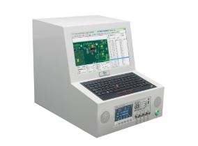
Our experienced engineers will assemble the first rapid PCB prototyping components by hand. The First Tester we independently researched and developed. Use this device to test the accuracy of the parameters of each component on the rapid PCB prototyping board that has been attached to the first piece. After testing, it will automatically generate a test report about the rapid Prototypeing board, and upload it to our MES, and take out a certificate to explain. This report will be sent to customers for confirmation and Check whether it meets the rapid PCB prototyping service standard. This product is independently developed by our company, and the industry is using our product. Finally, the first PCB assembly prototype will be functionally tested.
PCBasic has professional test engineers who can perform functional tests based on the test data provided by customers. This involves each rapid PCB prototyping assembly board and our engineers will also make test tools.
PCBasic can also provide customers with finished product assembly services, with mold and injection molding cooperation with original factories.
The QA personnel of the quality department make the final quality inspection link before the factory according to the tasks pushed by the MES and refer to the IPC610E standard.
Transport protection assessment. Before leaving the factory, the pictures are taken and uploaded to the MES for traceability.
We adopt the fastest way of logistics and distribution to ensure delivery.
PCBasic ensures that the products reach customers quickly and efficiently. We have the most advanced equipment, MES system, and IoT. Every rapid PCB prototyping assembly board is produced with advanced production technology, and it is perfect.
After the project is completed, we will create a complete document package, including BOM, Gerber files, and rapid PCB prototyping service technical manuals. In addition, we also set a warranty period for rapid PCB prototyping service. During this period, we will fix the error and provide other technical support within the warranty.
As the rapid PCB prototyping board are manufactured, we subject each PCB prototyping to strict test and check also when accomplished:
· E-Test
· Automated Optical Inspection
· X-ray
· CCD – Camera Controlled Drilling
· Impedance control
13 Steps PCBA Quality Testing
1. Prototype PCB Assembly Process Evaluation
2. IQC Incoming Inspection
3. Material Intelligent Warehousing
4. SPI ( Solder Paste Inspection)
5. Online AOI Detection
6. SMT First Article Inspection
7. IPQC Process Inspection
8. Offline AOI Detection
9. X-RAY Detection
10. QC Visual Inspection
11. Automatic Welding
12. Automatic Splitter
13. QA Final Inspection
PCBasic has its factory and has rich experience in rapid PCB Prototyping and Layout Design field for over 10 years. Professional rapid PCB prototyping service, the quality of PCB prototyping board is guaranteed. Additionally, we can save you time and money. We provide one-stop PCB prototype services, including rapid PCB prototyping and layout design, prototype PCB fabrication, component sourcing, prototype PCB assembly, and mold injection.
As a leading rapid PCB prototyping service company and prototype fabrication company, our PCB prototype designers are more than happy to serve our global customers with custom requirements to fulfill all your PCB prototype design needs.
Assembly Enquiry
Instant Quote
Phone contact

+86-755-27218592
In addition, we've prepared a Help Center. We recommend checking it before reaching out, as your question and its answer may already be clearly explained there.
Wechat Support

In addition, we've prepared a Help Center. We recommend checking it before reaching out, as your question and its answer may already be clearly explained there.
WhatsApp Support

In addition, we've prepared a Help Center. We recommend checking it before reaching out, as your question and its answer may already be clearly explained there.