Rigid PCBs are among the most crucial parts of any
electronic manufacturing process. Be it simple consumer electronics, medical
devices or more complex industrial systems, they have always been the ideal
solution.
One of the main reasons rigid circuit boards continue to
dominate the market up to date is because of their strength and versatility.
Read on as we take a more in-depth look at rigid PCBs, their
features, manufacturing process, and more.
Definition of a Rigid PCB
A rigid PCB is one of the most fascinating circuit board
types. Unlike flexible circuit boards that can bend and flex, rigid PCBs
feature rigid, solid structure – thanks to their rigorous composite material
composition.
At the core of every rigid PCB lies a rigid substrate
(usually a glass-epoxy laminate like FR4) which prevents any warping or
distortions. This allows rigid circuit boards to maintain their precise shape
and placement of components no matter the conditions. Topping this sturdy
substrate are meticulously etched layers of copper traces and pathways – each
one enabling critical electrical connections.
Encapsulating the whole assembly are protective coatings
like solder masks and identifying silkscreens. Once manufactured, rigid PCBs
lock their form forever – making them perfect for applications requiring
unyielding position and performance. Their design is also scalable from basic
single-layer forms to complexity of multilayer structuring with 6, 8 or 10+
finely-tuned layers.
Rigid circuit boards truly exemplify the balance of strength
and circuitry. Their resilience has made them central to domains like
computers, industrial machinery, aerospace technology and more.
Features of Rigid Circuit Boards
Rigid circuit boards offer a unique combination of
attributes that make them ideal for a wide range of demanding applications.
Here are some of their key features:
● Durability: Rigid circuit boards feature solid
substrates that provide inherent strength and rigidity. This durability makes
them resistant to flexing, twisting and warping over extended use in
challenging conditions. With no risk of component movement or breakage, rigid
boards maintain circuit integrity through countless power cycles.
● Heat dissipation: The solid construction of rigid
boards facilitates optimal heat dissipation compared to flexible boards. Their
copper layers efficiently distribute thermal loads across the board. This
optimized thermal performance allows rigid boards to reliably operate
electronics in high-temperature industrial environments that would damage less
robust board types.
● High-density circuitry: Rigid PCBs accommodate greatly
dense circuit design compared to flexible PCBs. Their rigidity holds tightly
packed components, interconnects and layer stacks in precise alignment. This
high-density capability maximizes functionality within minimal board space for
size-critical applications.
● Application versatility: From basic consumer electronics to
advanced aerospace systems, rigid PCBs excel in a vast array of sectors and
product types. Their design versatility supports anything from simple
singule-plate components to complex multilayer CPU architectures. This wide
application range stems from rigid boards' ideal balance of strength, thermal
performance and circuit complexity.
The Process of a Rigid PCB
Manufacture
The process of manufacturing a rigid PCB may seem like that
of a simple circuit board but it is not so. Unlike flex PCB manufacturing, it
involves a more rigorous process that requires more input.
These are the steps that are followed to make the final
product:
1.
Sheet Cutting
The process starts with copper-clad laminates which act as
the base material to the whole process. These laminates are usually of FR-4
fiberglass and can be several feet wide. The laminate sheets are then cut into
smaller panels of the size of the required PCB design with the help of a
precision computer-controlled cutting machine. Slicing knives scratch and tear
the material and provide the panel edges that are ready for further processing
and are clean and smooth.
2.
Laminating
In the case of multilayer boards, the inner layers have to
be made. Thin foil sheets are exposed to the layer’s circuit image through
photoresist imaging methods. Preg sheets – thin plies of fiberglass/epoxy – are
used to insulate the layers. The etched foils and prepregs are then aligned in
a suitable manner and then put into a vacuum lamination press. The materials
are heated and pressed together and the molecular bond is formed on the atomic
level to create a single rigid panel with multiple layers of circuits embedded
in it.
3.
Laser Drilling
Vias – plated holes that connect layers – are drilled through
the laminated stack by using a high powered UV laser that is controlled by the
PCB data files. It is possible to bore holes with an accuracy of a few
thousandths of an inch in diameter. The rapidly moving laser accurately
penetrates through each layer, which means that the connections between the
embedded circuit patterns are perfectly vertical.
4.
Imaging and Etching
For the outer layers, the photoresist is used and the
photomask film and UV light are used to pattern the photoresist before etching
of the copper. The exposed film is then washed off leaving behind the copper
layer. The panels are then placed in a ferric chloride etching solution to
remove any copper atoms that may be exposed in the panels. This exactly
outlines the circuit traces and features.
5.
Electroplating
Electrolytic copper deposition is used to increase thickness
of the traces and to copper fill the laser vias. When an electric current is
passed through an electrolyte bath, copper dissolved in the bath is deposited
on the prepared board surfaces. This enhances the connection between layers.
A thin layer of solder mask material in the form of sand is
then applied on the patterned copper surfaces by screening. It is then exposed
to UV light or heat where it undergoes a chemical reaction to make the coating
become hard. The solder mask also serves the purpose of preventing the copper
layer from oxidizing and getting damaged while at the same time allowing the
pads and traces to be visible for assembly.
7.
Plating
Immersion or electrolytic deposition is used to put surface
finishes to the exposed pads. HASL type of finish uses hot tin-lead solder
electrolyte while ENIG uses nickel and immersion gold. These shields expose
copper from corrosion and ensure proper soldering when the product is being
manufactured.
8.
Screen Printing
Solder masks are used to print labels, text and diagrams on
the silkscreen layer to pass information on the design. PCB designs are used to
create stencils that help in the placement of each printed character with a lot
of precision and uniformity.
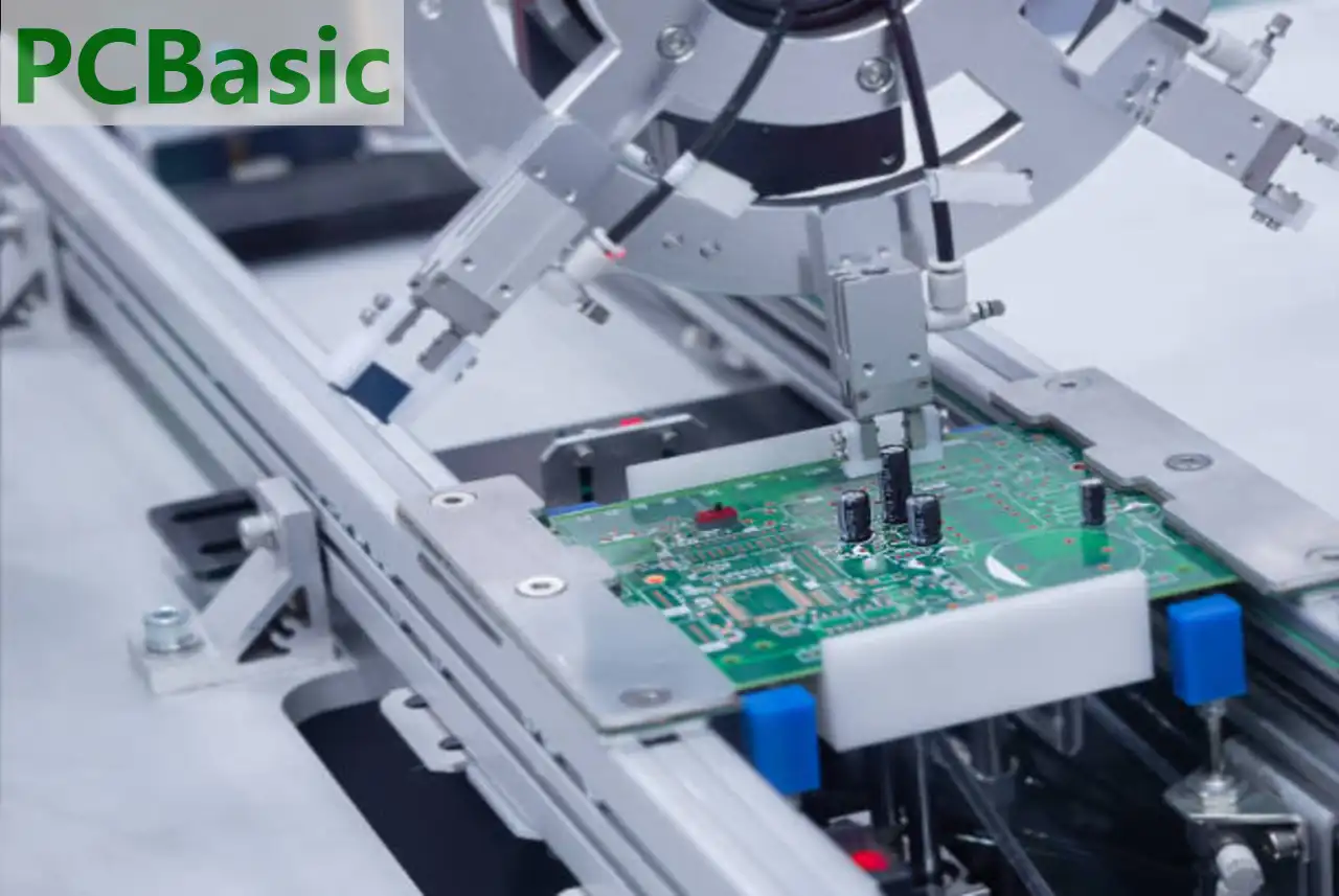
9.
Testing
Inline electrical tests are performed automatically with the
help of probe cards equipped with needles of a micrometric size. Computer
controlled systems check proper connectivity by passing signals through vias
and traces according to the netlist file created by the designer.
Any mistakes are indicative of problems from manufacturing
or design. Only those boards that are fully functional are able to pass this
important quality test.
10.
Final Routining
The finished boards are accurately shaped by CNC mills to
the final contour dimensions mentioned on the Gerber data files. High-speed
rapids spinning end-mills cut through layers with a microns accuracy leaving
edges clean and ready for assembly and integration.
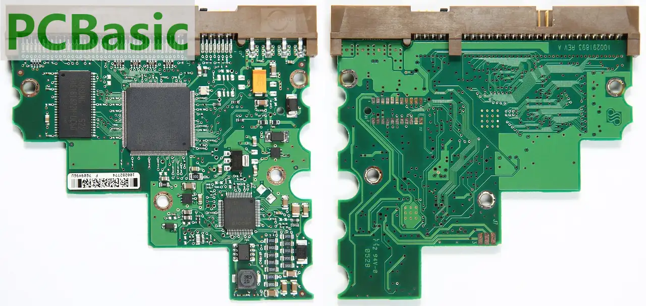
The building blocks of rigid printed circuit boards are the
various material layers that give the board its structure and function. There
are four fundamental layers - the substrate, copper, solder mask and silkscreen
layers.
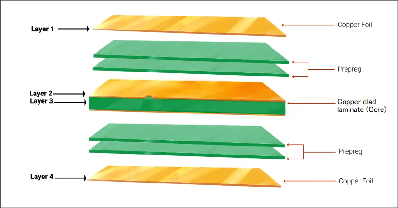
Substrate Layer
As the foundation, the substrate layer provides the board's
rigidity and rigidness. It is typically made of fiberglass reinforced epoxy
resin, commonly known as FR-4. FR-4 remains the most widely used substrate
material due its heat resistance, strength and affordability. Other options
include phenolic, polyimide and ceramic-based materials which offer enhanced
features but at a higher cost.
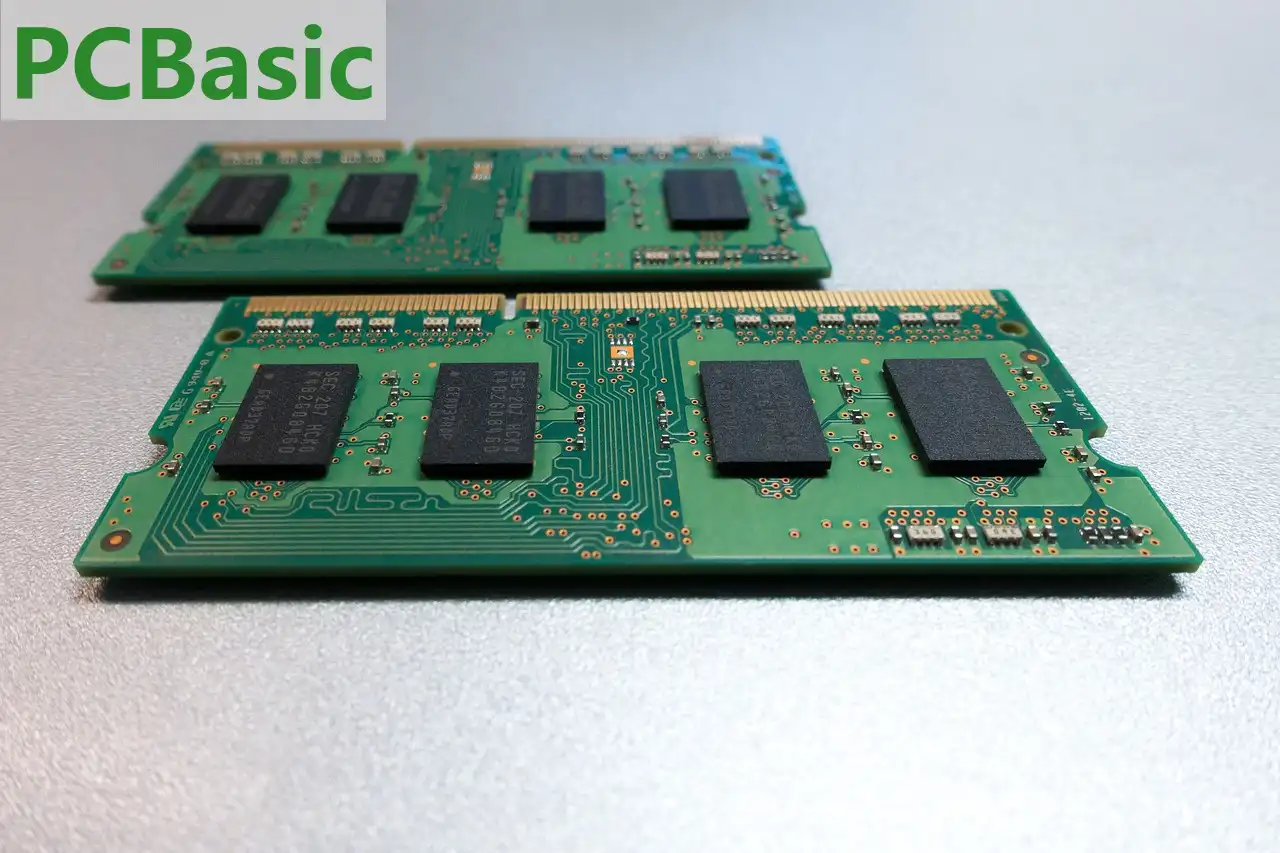
Copper Layer
Copper cladding is laminated on one or both sides of the
substrate to form the circuit pathways and connections. Copper is an excellent
conductor of electricity which allows signals and power to flow efficiently
across the board. For many applications, multiple inner copper layers may also
be added to the PCB stackup to create more complex circuit routing in less
board space.
Solder Mask Layer
Applied over the copper layer, solder mask serves several
critical roles. It protects and insulates the copper from corrosion and
oxidation. It also prevents solder bridges from forming between adjacent copper
traces during the assembly process. Solder mask is typically a digitally
printed coating that is heat cured onto the board.
Silkscreen Layer
This final layer prints the component designations,
manufacturer logos or other identifying text directly onto the surface of the
solder mask for easy identification. Silkscreened markings remain legible
throughout the lifetime of the PCB.
Applications of rigid PCBs
These are some of their most common
uses:
• Consumer Electronics: A large
number of devices that we constantly employ in our daily lives are based on the
use of rigid PCBs. All sorts of devices, such as computers, laptops, tablets,
mobile phones and others, have rigid boards for their internal wiring.
• Industrial Equipment: Since
rigid PCBs are controlled and fixed in form, they can be used in industrial
machinery. They are used in automation systems, medical devices such as MRI
machines, networking equipment, and many others.
• Automotive Electronics: The
environment of vehicles is very challenging and thus, the electronics used in
the vehicles must be robust and stable. Rigid PCBs are used in systems such as
dashboard computers, engine control modules, sensors, and many others.
• Aerospace Technology:
Conditions in planes and space vehicles are as bad as they can get. Rigid
panels withstand heat, vibrations, and stress and thus support avionic equipment,
sensors, communication equipment and so on.
• Heavy Machinery: As with
automotive, rigid PCBs can endure the harsh environment of the use of equipment
such as manufacturing tools. They are employed in industrial robots, 3D
printers, factory automation and many others.
• Appliances: Most household
appliances, such as washing machines, dishwashers, air conditioners, and more
are designed with rigid circuits to minimize failure. They are not very mobile,
which is good for stationary appliances.
Rigid vs flexible vs rigid-flex PCB
When developing a printed circuit board, one of the first
significant choices made is whether it will be rigid, flexible, or rigid-flex.
Both types have their unique characteristics that qualify them for specific
uses.
Durability and Strength
Rigid PCBs are the most robust and can withstand harsh
conditions as compared to the flexible ones. Manufactured from rigid fiberglass
or FR-4 material, they are heat, impact, and pressure resistant. However, their
construction is very rigid and they cannot bend or flex in any way.
Flexible PCBs are made from thin polyimide film and
therefore they are light in weight but soft and can easily be bent. However,
they are not as rigid and strong as rigid boards which are used in most
applications. Rigid-flex PCBs are a compromise – rigid parts offer structural
stability and the flexible sections can be bent.
Form Factor and Flexibility
Smartwatches, mobile phones, and products that have a
capability of being folded or can be made flexible need flexible or rigid-flex
designs. Only these options can be shaped to fit the contours of curves or bend
at hinges/joints.
Rigid PCBs are rigid – they do not bend or flex, they remain
flat and can’t be folded. Selecting flexible or rigid-flex allows you to have
much more freedom in designing beautiful and ergonomic enclosures that can also
follow the user.
Line Crosstalk and Noise
The signals passing through the rigid boards are least
disturbed and the interferences are very low. On flexible boards, lines which
are in close proximity to each other or intersecting at small angles can cause
noise or crosstalk.
Rigid-flex boards do this through rigid ‘islands’ that
contain noise sensitive components and signals in separate areas. If
noise/crosstalk is not an issue in your design, then basic single-sided
flexible circuits should be sufficient.
Cost and Complexity
Rigid-flex PCB costs more because its fabrication is more
complicated than rigid boards, and it uses chemical procedures. They are normally
more expensive per unit than other forms of packaging. Flex circuits also have
larger design margins and routing issues.
For basic, inexpensive layouts that do not call for
mechanical bending, rigid boards continue to be the least expensive option.
Materials and Environmental
Resistance
Rigid boards are usually made from fiberglass laminate
materials such as the FR-4 which has the capability of handling high
temperatures.
Flexible boards use polyimide film which has lower heat
resistance as compared to the epoxy glass fiber used in rigid boards.
Rigid-flex has the advantages of both the above mentioned technologies.
Flexible circuits also have low resistance to chemicals, moisture and corrosive
environment than the rigid circuits boards.
Component Density
Rigid boards enable higher component density because the
components do not require a larger separation as in flexible circuits. This
makes rigid best for applications that require a high density of components to
be accommodated in a given space. Flexible and rigid-flex have lower maximum
component densities than rigid.
Manufacturability
Rigid boards are usually less complex to manufacture than
the flexible or rigid-flex boards. Some of the characteristics such as plated
through holes, multi-layering and tight design requirements are easily
implemented on rigid PCBs. Flexible and rigid-flex fabrication involve
laminating, flex cutting and routing which are different from conventional
fabrication and add to the fabrication difficulty.
Conclusion
Rigid PCBs continue to be an indispensable part of
electronic manufacturing. Whether it's consumer electronics, automotive apps,
industrial machinery or aerospace systems – rigid boards provide the reliable
foundations for circuits of all kinds.
As technology grows ever more sophisticated, so do the
demands we place on PCBs. Manufacturers are constantly innovating to push the
limits of what's possible, from multi-layer complexity to nano-sized traces.
If you've got an electronics project in the works that could
benefit from a customized rigid PCB, PCBasic has got your back. Our team of engineers have decades of
experience crafting boards for all manner of applications. Best of all, we can
provide a prototype for you at an affordable price.
Simply contact us today to get started – it could move your
next innovation one step closer to reality.