Global high-mix volume high-speed PCBA manufacturer
9:00 -18:00, Mon. - Fri. (GMT+8)
9:00 -12:00, Sat. (GMT+8)
(Except Chinese public holidays)
Global high-mix volume high-speed PCBA manufacturer
9:00 -18:00, Mon. - Fri. (GMT+8)
9:00 -12:00, Sat. (GMT+8)
(Except Chinese public holidays)
HomePage > Blog > Knowledge Base > Power Supply PCB|A Comprehensive Guide
A power supply PCB is an essential component in almost all electronic devices. It provides the necessary voltage and current to power the circuit board. Power supply modules are designed to ensure that the power provided is stable, reliable, and compatible with the components of the system.
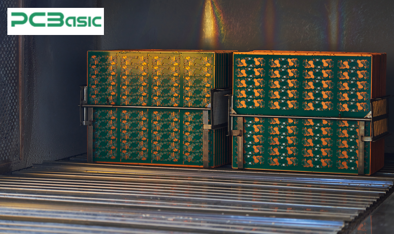
A power supply PCB is a printed circuit board specifically designed to supply electrical power to other components of an electronic device. These boards are responsible for converting high-voltage AC power into low-voltage DC power, ensuring that the correct amount of power is delivered to various components on the circuit board power supply.
Unlike standard PCBs, power supply circuit boards are designed to handle larger currents and often feature more robust components, such as transformers, rectifiers, and voltage regulators. They play a critical role in ensuring that electronic devices operate efficiently and safely.
Power supply boards are distinct from other types of PCBs, such as signal processing boards, because they focus primarily on power conversion and distribution.
The key components of a power supply PCB board include:
Power supply modules: These are the core elements that handle voltage conversion, such as buck converters, boost converters, or linear regulators.
Transformers: Used in power PCB designs, transformers help step up or step down the voltage to the desired level.
Rectifiers: These components convert AC to DC, a critical function in many power supplies.
Capacitors: In PCB power supply designs, capacitors are used for smoothing and filtering to reduce noise and ripple in the power output.
Inductors: These help manage current and reduce noise in power supplies.
Voltage regulators: These ensure that the voltage levels remain stable regardless of input voltage fluctuations or varying load conditions.
These components work together to ensure that the power supplied to a pcb mount power supply is stable and within the correct parameters for the device to function properly.
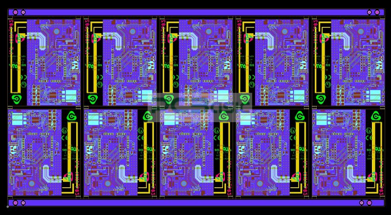
Designing a power supply PCB involves several key considerations to ensure efficient, stable, and safe power delivery. Power supply PCB design is crucial in preventing power-related issues like overheating, voltage instability, and electromagnetic interference (EMI).
When designing a power supply PCB, several key factors must be taken into account:
Power type: Whether using a linear power supply or a switch-mode power supply, the design will vary greatly depending on the power requirements and efficiency needs.
Thermal management: Effective heat dissipation is critical, especially for high-power designs, to prevent overheating.
Power integrity (PI): Ensuring stable and clean power delivery to all components to prevent malfunction.
EMI suppression: Minimizing electromagnetic interference to meet regulatory standards.
Choosing the right power PCB design type depends largely on the application and the type of power conversion needed. Common power supply designs include:
Linear power supplies: Simple but less efficient; suitable for applications where low noise is crucial.
Switch-mode power supplies (SMPS): More efficient, capable of handling higher power, and typically used in applications requiring high efficiency and compact designs.
When selecting the appropriate power supply design, it's essential to consider factors such as power efficiency, size limitations, cost, and the type of device being powered.
To create an efficient and reliable power supply PCB design, the following best practices should be followed:
The choice between linear regulators and switching regulators will largely depend on the specific power requirements:
Linear regulators are ideal for low-noise, low-power applications where the power conversion efficiency is not a top priority.
Switching regulators are more efficient for higher power applications and can handle larger input-to-output voltage variations.
It's important to choose the regulator that best matches the load and efficiency requirements of your pcb power supply.
Thermal management is a critical aspect of power supply PCB design. Components such as voltage regulators, power transistors, and transformers can generate significant heat, which, if not managed properly, could cause failure or damage to the circuit board. Some thermal management strategies include:
Using heat sinks or thermal vias to dissipate heat.
Proper component placement to ensure adequate airflow.
Selecting components that have lower heat generation.
Ensuring proper heat dissipation will help maintain the stability and longevity of the power supply PCB.
Bypassing and decoupling capacitors are used in power supply PCB design to filter out high-frequency noise and smooth the power supply. These capacitors are strategically placed to prevent unwanted noise from affecting sensitive components on the pcb power supply.
Bypass capacitors help reduce power noise and fluctuations.
Decoupling capacitors ensure stable voltage at the power supply inputs to sensitive circuits.
By properly implementing these components, the design can avoid common power integrity issues, ensuring the overall stability of the power supply circuit board.
EMI suppression is crucial in power PCB designs to prevent electromagnetic interference that can disrupt the operation of nearby electronics. Some strategies include:
Adding filtering components such as ferrite beads, inductors, and capacitors.
Implementing shielding and grounding techniques to isolate noise sources.
EMI suppression not only improves device performance but also ensures compliance with industry standards and regulations for power supply board designs.
Switching regulators, while efficient, can generate significant EMI. Effective shielding can help minimize this interference. Techniques such as:
Using shielded enclosures for sensitive components.
Ground planes on the PCB to reduce noise.
Filtered inputs/outputs to prevent noise from traveling through the power supply.
By incorporating shielding techniques, designers can mitigate the risks associated with EMI, ensuring that the power supply PCB board meets performance and regulatory standards.
Designing the layout for a power supply PCB requires careful consideration of several factors to ensure that the power distribution is efficient, stable, and free from interference. This section covers key aspects of power supply circuit board layout, including the differences between linear and switch-mode power supplies, as well as guidelines for grounding, trace conductivity, component placement, trace routing, and thermal management.
When designing a PCB power supply, it's important to understand the differences between linear and switch-mode power supplies (SMPS), as these two designs have different layout requirements.
Linear Power Supplies: Linear regulators are simpler to design but less efficient because they dissipate excess voltage as heat. This means that the power supply board for a linear power supply requires careful attention to heat management. Linear regulators typically have lower EMI (electromagnetic interference), making them suitable for applications requiring low-noise power.
Switch Mode Power Supplies (SMPS): SMPS designs are more complex but highly efficient, converting power through a switching process. However, SMPS can generate significant EMI, requiring careful routing and shielding in the power PCB to avoid noise coupling into other components. Additionally, switch-mode power supplies usually have higher efficiency, but the design must account for heat dissipation due to higher power densities.
Both designs require attention to power supply PCB design principles but differ in their requirements for managing noise, heat, and power efficiency.
A power supply PCB board layout must ensure that the power is delivered effectively while minimizing issues such as noise, heat generation, and power loss. The following guidelines help optimize the layout for both functionality and performance.
Grounding is one of the most critical aspects of power supply PCB design. A good grounding system helps reduce noise and interference, especially in circuit board power supply designs. Proper grounding techniques include:
Creating a ground plane on the PCB to provide a low-resistance return path for current.
Using multiple ground layers or islands for sensitive signal paths to isolate noise.
Minimizing the path between power components and their ground connections to reduce inductance and resistance.
A solid grounding design will help minimize EMI and improve the stability of the pcb power supply.
Choosing the right trace width is essential for ensuring that the power supply PCB can handle the required current without overheating. The trace width depends on the current requirements and the allowable temperature rise. To determine the correct trace width:
Use PCB power supply design calculators or formulas to determine the necessary width based on the current and copper thickness.
Consider using wider traces for high-current paths, such as those leading to power supply modules or high-power components.
Ensure that the trace conductivity is sufficient to prevent voltage drops and ensure power integrity.
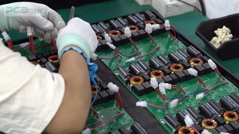
Effective component placement is key to optimizing the performance of a power supply PCB board. Components must be arranged to minimize signal path lengths, reduce interference, and ensure efficient heat dissipation. Key considerations include:
Place high-current components, such as voltage regulators and power transistors, near the power input to minimize voltage drops.
Keep sensitive components, such as microcontrollers or op-amps, away from noisy power components to avoid interference.
Position components based on their thermal performance to optimize heat flow and prevent overheating.
By properly placing components, you can improve the overall functionality and lifespan of the pcb mount power supply.
The way you route traces on a power PCB has a direct impact on the performance of the power supply. Important considerations for routing traces include:
Minimizing the length of high-current paths to reduce resistive losses and noise.
Avoiding routing high-current paths near sensitive signal traces to prevent EMI coupling.
Using power planes where possible to minimize the number of routing layers and reduce inductive effects.
Keeping high-frequency switching paths as short as possible to minimize EMI.
Proper trace routing ensures that the power supply circuit board maintains signal integrity and minimizes noise.
Thermal management is crucial for power supply PCB design, especially when designing for high-power applications. To ensure that your power supply PCB does not overheat:
Use heat sinks or thermal vias to dissipate heat away from high-power components.
Place power components such as voltage regulators and diodes in areas with good airflow.
Consider fan-assisted cooling or even active thermal management if the power density is very high.
Ensure there is enough spacing between components to allow for proper airflow and cooling.
Effective thermal management prevents thermal runaway and extends the life of your power supply modules.
Designing a power supply PCB is a complex process, and several factors must be carefully considered to ensure the power supply is efficient, reliable, and operates within safe thermal limits. These considerations include choosing the right voltage regulators, managing heat, addressing EMI, ensuring power integrity, and properly implementing decoupling capacitors.
Choosing the correct voltage regulator for a power PCB design is essential for meeting the voltage and current needs of the circuit. When selecting a voltage regulator, consider:
Output voltage and current requirements: Ensure the regulator can provide the necessary output power.
Efficiency: For high-efficiency designs, consider switching regulators over linear regulators.
Thermal performance: Ensure the regulator can operate within the thermal limits of the design.
Choosing the appropriate regulator ensures that the power supply board delivers stable and reliable power to all components.
Effective thermal management in power PCB designs ensures that the system operates at the correct temperature and prevents overheating. Strategies for thermal management include:
Using heat sinks on high-power components like regulators or transistors.
Implementing thermal vias to direct heat away from hot components.
Considering active cooling options for high-power systems.
Thermal management is crucial for ensuring that your power supply modules operate within safe temperature ranges, preventing failure or reduced performance.
EMI filtering is essential in power supply PCB design to prevent electromagnetic interference that can affect the performance of nearby circuits. Common techniques for EMI filtering include:
Using filtering components like inductors, capacitors, and ferrite beads.
Employing shielding to isolate sensitive components from high-power circuits.
Designing EMI filters that block unwanted high-frequency signals from the power supply.
By properly filtering EMI, you can improve the performance and reliability of your power supply circuit board.
Decoupling and bypass capacitors are used to ensure stable voltage and power delivery in power supply PCB design. These capacitors help:
Smooth out voltage fluctuations and eliminate high-frequency noise.
Provide a stable power source for sensitive components, ensuring power integrity (PI).
By strategically placing these capacitors, you can prevent power noise and improve the performance of the power supply PCB board.
Power integrity (PI) refers to the ability of a PCB power supply to deliver stable and noise-free power to all components. Key factors influencing PI include:
Proper grounding and trace routing to minimize voltage drops and noise.
Careful selection of capacitors to ensure stable power delivery.
EMI shielding to prevent noise from interfering with sensitive circuits.
Ensuring power integrity is vital for the reliable performance of the power PCB and the overall stability of the system.
When designing a power supply PCB, it is essential to address several key concerns to ensure the board performs well and meets all specifications. These concerns include addressing design guidelines, considering efficiency and cost, and selecting appropriate materials for production.
Some common challenges in power supply PCB design include:
Ensuring adequate thermal management to prevent overheating.
Proper trace width and component placement to ensure power is efficiently distributed.
Managing electromagnetic interference to meet regulatory requirements.
These guidelines help ensure that power supply PCB boards are designed for both performance and cost-efficiency.
Key concerns when designing power supply PCB boards include:
Power stability: Ensuring that the power supply modules provide reliable power under all conditions.
Efficiency: Maximizing the efficiency of the power conversion while minimizing losses.
Size constraints: Designing a compact board that fits within the size limitations of the device.
Cost control: Keeping costs low by using cost-effective components and optimizing the design.
Factors that influence the price of a power supply PCB include:
Material costs: High-quality copper or specialized PCB materials can increase costs.
Manufacturing complexity: More complex designs with multiple layers or components increase production costs.
Volume: Bulk production often leads to reduced costs.
In summary, designing a power supply PCB requires careful planning and attention to detail across various aspects, including voltage regulation, thermal management, power integrity, and EMI suppression. By following best practices for grounding, trace routing, and component placement, designers can ensure the power supply is stable, efficient, and reliable. Key considerations, such as selecting the right voltage regulators, managing heat, and reducing electromagnetic interference, will help deliver a high-performance power supply circuit board that meets the needs of the application.

Assembly Enquiry
Instant Quote
Phone contact

+86-755-27218592
In addition, we've prepared a Help Center. We recommend checking it before reaching out, as your question and its answer may already be clearly explained there.
Wechat Support

In addition, we've prepared a Help Center. We recommend checking it before reaching out, as your question and its answer may already be clearly explained there.
WhatsApp Support

In addition, we've prepared a Help Center. We recommend checking it before reaching out, as your question and its answer may already be clearly explained there.